Electrical characteristics
STM32F405xx, STM32F407xx
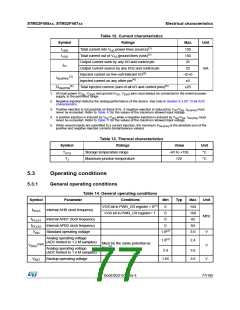
Table 14. General operating conditions (continued)
Symbol
Parameter
Conditions
Min
Typ
Max
Unit
VOS bit in PWR_CR register = 0(1)
Max frequency 144MHz
1.08
1.14
1.20
V
Regulator ON:
1.2 V internal voltage on
VCAP_1/VCAP_2 pins
VOS bit in PWR_CR register= 1
Max frequency 168MHz
1.20
1.10
1.26
1.14
1.32
1.20
V
V
V12
Regulator OFF:
Max frequency 144MHz
1.2 V external voltage must be
supplied from external regulator
on VCAP_1/VCAP_2 pins
Max frequency 168MHz
1.20
1.26
1.30
V
2 V ≤ VDD ≤ 3.6 V
VDD ≤ 2 V
–0.3
–0.3
-
-
5.5
5.2
Input voltage on RST and FT
pins(6)
VIN
V
VDDA
0.3
+
Input voltage on TTa pins
Input voltage on B pin
–0.3
-
-
5.5
435
465
500
526
513
543
85
LQFP64
-
-
LQFP100
Power dissipation at TA = 85 °C
for suffix 6 or TA = 105 °C for
suffix 7(7)
LQFP144
-
PD
mW
LQFP176
-
UFBGA176
-
WLCSP90
-
Maximum power dissipation
Low power dissipation(8)
Maximum power dissipation
Low power dissipation(8)
6 suffix version
7 suffix version
–40
–40
–40
–40
–40
–40
Ambient temperature for 6 suffix
version
°C
°C
°C
105
105
125
105
125
TA
TJ
Ambient temperature for 7 suffix
version
Junction temperature range
1. The average expected gain in power consumption when VOS = 0 compared to VOS = 1 is around 10% for the whole
temperature range, when the system clock frequency is between 30 and 144 MHz.
2. VDD/VDDA minimum value of 1.7 V is obtained when the device operates in reduced temperature range, and with the use of
an external power supply supervisor (refer to Section : Internal reset OFF).
3. When the ADC is used, refer to Table 67: ADC characteristics.
4. If VREF+ pin is present, it must respect the following condition: VDDA-VREF+ < 1.2 V.
5. It is recommended to power VDD and VDDA from the same source. A maximum difference of 300 mV between VDD and
V
DDA can be tolerated during power-up and power-down operation.
6. To sustain a voltage higher than VDD+0.3, the internal pull-up and pull-down resistors must be disabled.
7. If TA is lower, higher PD values are allowed as long as TJ does not exceed TJmax
8. In low power dissipation state, TA can be extended to this range as long as TJ does not exceed TJmax
.
.
78/185
DocID022152 Rev 4

 STMICROELECTRONICS [ ST ]