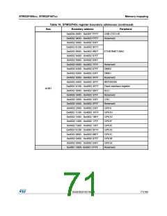
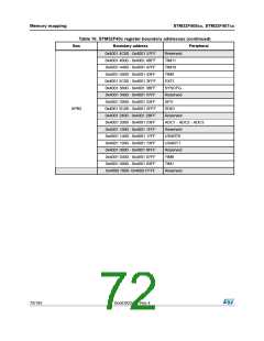
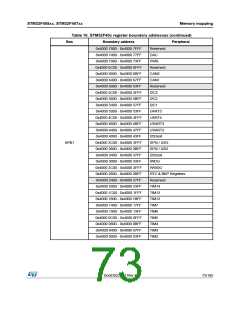
STM32F405xx, STM32F407xx
Electrical characteristics
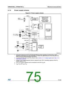
5.1.6
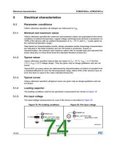
Power supply scheme
Figure 21. Power supply scheme
VBAT
Backup circuitry
VBAT =
1.65 to 3.6V
(OSC32K,RTC,
Wakeup logic
Power
switch
Backup registers,
backup RAM)
OUT
IN
IO
Logic
GPIOs
VCAP_1
VCAP_2
Kernel logic
(CPU, digital
& RAM)
2 × 2.2 μF
VDD
VDD
1/2/...14/15
Voltage
regulator
15 × 100 nF
+ 1 × 4.7 μF
VSS
1/2/...14/15
Flash memory
BYPASS_REG
PDR_ON
VDDA
Reset
controller
VDD
VREF
VREF+
Analog:
RCs,
PLL,..
100 nF
+ 1 μF
100 nF
+ 1 μF
ADC
VREF-
VSSA
MS19911V2
1. Each power supply pair must be decoupled with filtering ceramic capacitors as shown above. These
capacitors must be placed as close as possible to, or below, the appropriate pins on the underside of the
PCB to ensure the good functionality of the device.
2. To connect BYPASS_REG and PDR_ON pins, refer to Section 2.2.16: Voltage regulator and Table 2.2.15:
Power supply supervisor.
3. The two 2.2 µF ceramic capacitors should be replaced by two 100 nF decoupling capacitors when the
voltage regulator is OFF.
4. The 4.7 µF ceramic capacitor must be connected to one of the VDD pin.
5. VDDA=VDD and VSSA=VSS
.
DocID022152 Rev 4
75/185

 STMICROELECTRONICS [ ST ]