STM32F405xx, STM32F407xx
Description
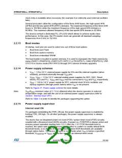
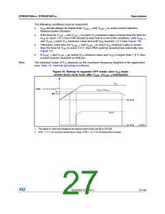
The following conditions must be respected:
•
V
should always be higher than V
and V
to avoid current injection
CAP_2
DD
CAP_1
between power domains.
•
If the time for V and V
to reach V minimum value is faster than the time for
CAP_1
CAP_2
12
V
to reach 1.8 V, then PA0 should be kept low to cover both conditions: until V
DD
CAP_1
and V
reach V minimum value and until V reaches 1.8 V (see Figure 10).
12 DD
CAP_2
•
•
Otherwise, if the time for V
and V
to reach V minimum value is slower
CAP_2 12
CAP_1
than the time for V to reach 1.8 V, then PA0 could be asserted low externally (see
DD
Figure 11).
If V
and V
go below V minimum value and V is higher than 1.8 V, then
CAP_1
CAP_2 12 DD
a reset must be asserted on PA0 pin.
Note:
The minimum value of V depends on the maximum frequency targeted in the application
12
(see Table 14: General operating conditions).
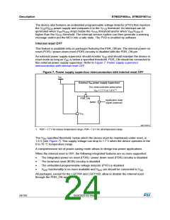
Figure 10. Startup in regulator OFF mode: slow V slope
DD
- power-down reset risen after V
/V
stabilization
CAP_1 CAP_2
VDD
PDR = 1.7 V or 1.8 V (2)
VCAP_1/VCAP_2
V12
Min V12
time
NRST
ai18491e
time
1. This figure is valid both whatever the internal reset mode (onON or OFFoff).
2. PDR = 1.7 V for reduced temperature range; PDR = 1.8 V for all temperature ranges.
DocID022152 Rev 4
27/185

 STMICROELECTRONICS [ ST ]