STM32F405xx, STM32F407xx
Description
clock entry is available when necessary (for example if an indirectly used external oscillator
fails).
Several prescalers allow the configuration of the three AHB buses, the high-speed APB
(APB2) and the low-speed APB (APB1) domains. The maximum frequency of the three AHB
buses is 168 MHz while the maximum frequency of the high-speed APB domains is
84 MHz. The maximum allowed frequency of the low-speed APB domain is 42 MHz.
The devices embed a dedicated PLL (PLLI2S) which allows to achieve audio class
2
performance. In this case, the I S master clock can generate all standard sampling
frequencies from 8 kHz to 192 kHz.
2.2.13
Boot modes
At startup, boot pins are used to select one out of three boot options:
•
•
•
Boot from user Flash
Boot from system memory
Boot from embedded SRAM
The boot loader is located in system memory. It is used to reprogram the Flash memory by
using USART1 (PA9/PA10), USART3 (PC10/PC11 or PB10/PB11), CAN2 (PB5/PB13), USB
OTG FS in Device mode (PA11/PA12) through DFU (device firmware upgrade).
2.2.14
Power supply schemes
•
•
•
V
= 1.8 to 3.6 V: external power supply for I/Os and the internal regulator (when
DD
enabled), provided externally through V pins.
DD
V
, V
= 1.8 to 3.6 V: external analog power supplies for ADC, DAC, Reset
DDA
SSA
blocks, RCs and PLL. V
and V
must be connected to V and V , respectively.
DDA
SSA DD SS
V
= 1.65 to 3.6 V: power supply for RTC, external clock 32 kHz oscillator and
BAT
backup registers (through power switch) when V is not present.
DD
Refer to Figure 21: Power supply scheme for more details.
V /V minimum value of 1.7 V is obtained when the device operates in reduced
DD DDA
Note:
temperature range, and with the use of an external power supply supervisor (refer to
Section : Internal reset OFF).
Refer to Table 2 in order to identify the packages supporting this option.
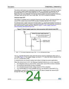
2.2.15
Power supply supervisor
Internal reset ON
On packages embedding the PDR_ON pin, the power supply supervisor is enabled by
holding PDR_ON high. On all other packages, the power supply supervisor is always
enabled.
The device has an integrated power-on reset (POR) / power-down reset (PDR) circuitry
coupled with a Brownout reset (BOR) circuitry. At power-on, POR/PDR is always active and
ensures proper operation starting from 1.8 V. After the 1.8 V POR threshold level is
reached, the option byte loading process starts, either to confirm or modify default BOR
threshold levels, or to disable BOR permanently. Three BOR thresholds are available
through option bytes. The device remains in reset mode when V is below a specified
DD
threshold, V
or V
, without the need for an external reset circuit.
POR/PDR
BOR
DocID022152 Rev 4
23/185

 STMICROELECTRONICS [ ST ]