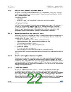
Description
STM32F405xx, STM32F407xx
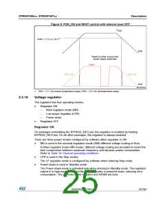
Two external ceramic capacitors should be connected on V
& V
pin. Refer to
CAP_1
CAP_2
Figure 21: Power supply scheme and Figure 16: VCAP_1/VCAP_2 operating conditions.
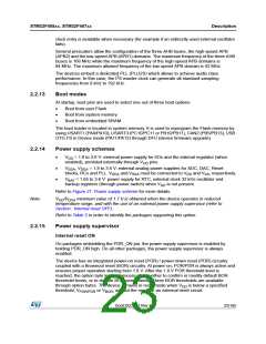
All packages have regulator ON feature.
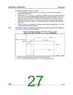
Regulator OFF
This feature is available only on packages featuring the BYPASS_REG pin. The regulator is
disabled by holding BYPASS_REG high. The regulator OFF mode allows to supply
externally a V voltage source through V
and V
pins.
12
CAP_1
CAP_2
Since the internal voltage scaling is not manage internally, the external voltage value must
be aligned with the targetted maximum frequency. Refer to Table 14: General operating
conditions.
The two 2.2 µF ceramic capacitors should be replaced by two 100 nF decoupling
capacitors.
Refer to Figure 21: Power supply scheme
When the regulator is OFF, there is no more internal monitoring on V . An external power
12
supply supervisor should be used to monitor the V of the logic power domain. PA0 pin
12
should be used for this purpose, and act as power-on reset on V power domain.
12
In regulator OFF mode the following features are no more supported:
•
PA0 cannot be used as a GPIO pin since it allows to reset a part of the V logic power
domain which is not reset by the NRST pin.
12
•
As long as PA0 is kept low, the debug mode cannot be used under power-on reset. As
a consequence, PA0 and NRST pins must be managed separately if the debug
connection under reset or pre-reset is required.
Figure 9. Regulator OFF
V12
External VCAP_1/2 power
Application reset
supply supervisor
signal (optional)
Ext. reset controller active
when VCAP_1/2 < Min V12
VDD
PA0
VDD
NRST
BYPASS_REG
V12
VCAP_1
VCAP_2
ai18498V4
26/185
DocID022152 Rev 4

 STMICROELECTRONICS [ ST ]