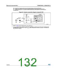
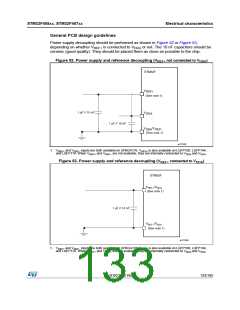
Electrical characteristics
STM32F405xx, STM32F407xx
Comments
Table 74. DAC characteristics (continued)
Symbol
Parameter
Min Typ
Max
Unit
DAC_OUT Lower DAC_OUT voltage
-
-
0.5
-
-
mV
min(2)
with buffer OFF
It gives the maximum output
excursion of the DAC.
DAC_OUT Higher DAC_OUT voltage
V
REF+ – 1LSB
V
max(2)
with buffer OFF
With no load, worst code (0x800)
at VREF+ = 3.6 V in terms of DC
consumption on the inputs
-
170
240
DAC DC VREF current
consumption in quiescent
mode (Standby mode)
(4)
IVREF+
µA
µA
With no load, worst code (0xF1C)
at VREF+ = 3.6 V in terms of DC
consumption on the inputs
-
-
-
50
75
With no load, middle code (0x800)
on the inputs
280
475
380
625
DAC DC VDDA current
consumption in quiescent
mode(3)
(4)
IDDA
With no load, worst code (0xF1C)
µA at VREF+ = 3.6 V in terms of DC
consumption on the inputs
Given for the DAC in 10-bit
configuration.
-
-
±0.5
LSB
Differential non linearity
Difference between two
consecutive code-1LSB)
DNL(4)
Given for the DAC in 12-bit
configuration.
-
-
-
-
±2
±1
LSB
Integral non linearity
(difference between
Given for the DAC in 10-bit
configuration.
LSB
measured value at Code i
and the value at Code i on a
line drawn between Code 0
and last Code 1023)
INL(4)
Given for the DAC in 12-bit
configuration.
-
-
±4
LSB
Given for the DAC in 12-bit
configuration
-
-
-
-
-
-
-
-
±10
±3
mV
Offset error
(difference between
measured value at Code
(0x800) and the ideal value
= VREF+/2)
Given for the DAC in 10-bit at
VREF+ = 3.6 V
Offset(4)
LSB
Given for the DAC in 12-bit at
LSB
±12
±0.5
VREF+ = 3.6 V
Gain
Given for the DAC in 12-bit
configuration
Gain error
%
µs
dB
error(4)
Settling time (full scale: for a
10-bit input code transition
between the lowest and the
highest input codes when
DAC_OUT reaches final
value ±4LSB
CLOAD ≤ 50 pF,
RLOAD ≥ 5 kΩ
(4)
tSETTLING
-
-
3
-
6
-
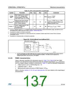
Total Harmonic Distortion
Buffer ON
CLOAD ≤ 50 pF,
RLOAD ≥ 5 kΩ
THD(4)
136/185
DocID022152 Rev 4

 STMICROELECTRONICS [ ST ]