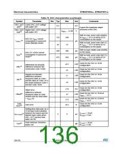
Electrical characteristics
STM32F405xx, STM32F407xx
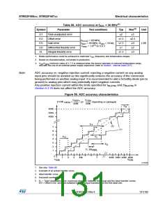
EG = Gain Error: deviation between the last ideal transition and the last actual one.
ED = Differential Linearity Error: maximum deviation between actual steps and the ideal one.
EL = Integral Linearity Error: maximum deviation between any actual transition and the end point
correlation line.
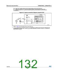
Figure 51. Typical connection diagram using the ADC
STM32F
V
DD
Sample and hold ADC
V
0.6 V
T
converter
(1)
C
(1)
R
R
AIN
ADC
AINx
12-bit
converter
V
T
V
AIN
0.6 V
C
(1)
ADC
parasitic
I
1 µA
L
ai17534
1. Refer to Table 67 for the values of RAIN, RADC and CADC
.
2. Cparasitic represents the capacitance of the PCB (dependent on soldering and PCB layout quality) plus the
pad capacitance (roughly 5 pF). A high Cparasitic value downgrades conversion accuracy. To remedy this,
fADC should be reduced.
132/185
DocID022152 Rev 4

 STMICROELECTRONICS [ ST ]