Electrical characteristics
Symbol
STM32F405xx, STM32F407xx
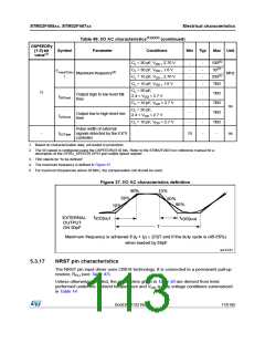
Table 50. NRST pin characteristics
Parameter
Conditions
Min
Typ
Max
Unit
(1)
VIL(NRST)
NRST Input low level voltage
NRST Input high level voltage
NRST Input low level voltage
NRST Input high level voltage
TTL ports
2.7 V ≤ VDD
≤ 3.6 V
-
-
-
0.8
(1)
VIH(NRST)
2
-
-
V
(1)
VIL(NRST)
CMOS ports
1.8 V ≤ VDD
≤ 3.6 V
0.3VDD
-
(1)
VIH(NRST)
0.7VDD
NRST Schmitt trigger voltage
hysteresis
Vhys(NRST)
RPU
-
200
-
mV
Weak pull-up equivalent resistor(2)
VIN = VSS
30
-
40
-
50
100
-
kΩ
ns
ns
(1)
VF(NRST)
NRST Input filtered pulse
(1)
VNF(NRST)
NRST Input not filtered pulse
VDD > 2.7 V
300
-
Internal
Reset source
TNRST_OUT Generated reset pulse duration
20
-
-
µs
1. Guaranteed by design, not tested in production.
2. The pull-up is designed with a true resistance in series with a switchable PMOS. This PMOS contribution to
the series resistance must be minimum (~10% order).
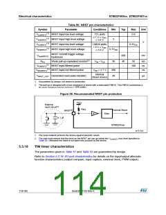
Figure 38. Recommended NRST pin protection
V
DD
External
reset circuit
(1)
R
PU
(2)
Internal Reset
STM32Fxxx
NRST
Filter
0.1 μF
ai14132c
1. The reset network protects the device against parasitic resets.
2. The user must ensure that the level on the NRST pin can go below the VIL(NRST) max level specified in
Table 50. Otherwise the reset is not taken into account by the device.
5.3.18
TIM timer characteristics
The parameters given in Table 51 and Table 52 are guaranteed by design.
Refer to Section 5.3.16: I/O port characteristics for details on the input/output alternate
function characteristics (output compare, input capture, external clock, PWM output).
114/185
DocID022152 Rev 4

 STMICROELECTRONICS [ ST ]