STM32F405xx, STM32F407xx
Electrical characteristics
In the user application, the number of I/O pins which can drive current must be limited to
respect the absolute maximum rating specified in Section 5.2. In particular:
•
The sum of the currents sourced by all the I/Os on V
plus the maximum Run
DD,
consumption of the MCU sourced on V
cannot exceed the absolute maximum rating
DD,
I
(see Table 12).
VDD
•
The sum of the currents sunk by all the I/Os on V plus the maximum Run
SS
consumption of the MCU sunk on V cannot exceed the absolute maximum rating
SS
I
(see Table 12).
VSS
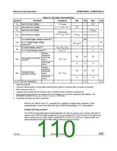
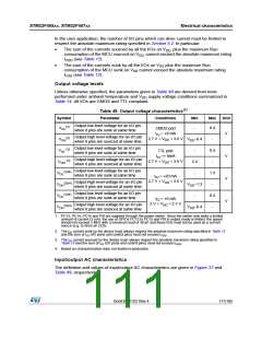
Output voltage levels
Unless otherwise specified, the parameters given in Table 48 are derived from tests
performed under ambient temperature and V supply voltage conditions summarized in
DD
Table 14. All I/Os are CMOS and TTL compliant.
(1)
Table 48. Output voltage characteristics
Symbol
Parameter
Conditions
Min
Max
Unit
Output low level voltage for an I/O pin
when 8 pins are sunk at same time
(2)
VOL
-
0.4
CMOS port
IIO = +8 mA
V
Output high level voltage for an I/O pin
when 8 pins are sourced at same time
(3)
2.7 V < VDD < 3.6 V
VOH
VDD–0.4
-
0.4
-
Output low level voltage for an I/O pin
when 8 pins are sunk at same time
(2)
VOL
-
2.4
-
TTL port
IIO =+ 8mA
V
V
V
Output high level voltage for an I/O pin
when 8 pins are sourced at same time
(3)
2.7 V < VDD < 3.6 V
VOH
Output low level voltage for an I/O pin
when 8 pins are sunk at same time
(2)(4)
VOL
1.3
-
IIO = +20 mA
2.7 V < VDD < 3.6 V
Output high level voltage for an I/O pin
when 8 pins are sourced at same time
(3)(4)
VOH
V
DD–1.3
-
VDD–0.4
Output low level voltage for an I/O pin
when 8 pins are sunk at same time
(2)(4)
VOL
0.4
-
IIO = +6 mA
2 V < VDD < 2.7 V
Output high level voltage for an I/O pin
when 8 pins are sourced at same time
(3)(4)
VOH
1. PC13, PC14, PC15 and PI8 are supplied through the power switch. Since the switch only sinks a limited
amount of current (3 mA), the use of GPIOs PC13 to PC15 and PI8 in output mode is limited: the speed
should not exceed 2 MHz with a maximum load of 30 pF and these I/Os must not be used as a current
source (e.g. to drive an LED).
2. The IIO current sunk by the device must always respect the absolute maximum rating specified in Table 12
and the sum of IIO (I/O ports and control pins) must not exceed IVSS
.
3. The IIO current sourced by the device must always respect the absolute maximum rating specified in
Table 12 and the sum of IIO (I/O ports and control pins) must not exceed IVDD
.
4. Based on characterization data, not tested in production.
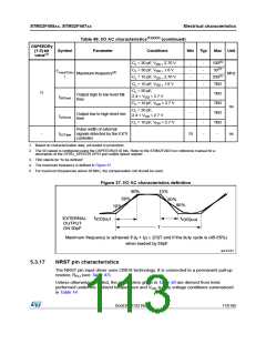
Input/output AC characteristics
The definition and values of input/output AC characteristics are given in Figure 37 and
Table 49, respectively.
DocID022152 Rev 4
111/185

 STMICROELECTRONICS [ ST ]