STM32F405xx, STM32F407xx
Electrical characteristics
(1)(2)(3)
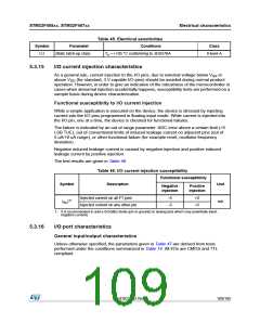
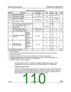
Table 49. I/O AC characteristics
(continued)
OSPEEDRy
[1:0] bit
Symbol
Parameter
Conditions
Min
Typ
Max Unit
value(1)
CL = 30 pF, VDD > 2.70 V
CL = 30 pF, VDD > 1.8 V
CL = 10 pF, VDD > 2.70 V
CL = 10 pF, VDD > 1.8 V
-
-
-
-
-
-
-
-
100(5)
50(5)
MHz
Fmax(IO)ou
Maximum frequency(4)
200(5)
t
TBD
TBD
CL = 20 pF,
11
-
-
-
-
-
-
-
-
Output high to low level fall
time
2.4 < VDD < 2.7 V
tf(IO)out
CL = 10 pF, VDD > 2.7 V
TBD
ns
CL = 20 pF,
TBD
Output low to high level rise
time
2.4 < VDD < 2.7 V
tr(IO)out
CL = 10 pF, VDD > 2.7 V
TBD
Pulse width of external
-
tEXTIpw signals detected by the EXTI
controller
10
-
-
ns
1. Based on characterization data, not tested in production.
2. The I/O speed is configured using the OSPEEDRy[1:0] bits. Refer to the STM32F20/21xxx reference manual for a
description of the GPIOx_SPEEDR GPIO port output speed register.
3. TBD stands for “to be defined”.
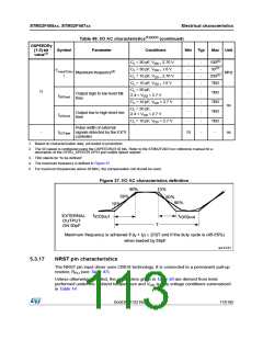
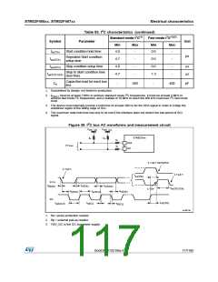
4. The maximum frequency is defined in Figure 37.
5. For maximum frequencies above 50 MHz, the compensation cell should be used.
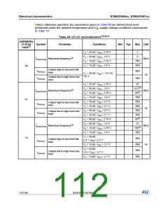
Figure 37. I/O AC characteristics definition
90%
10%
50%
50%
10%
90%
t
t
EXTERNAL
OUTPUT
ON 50pF
r(IO)out
r(IO)out
T
Maximum frequency is achieved if (t + t ) ≤ 2/3)T and if the duty cycle is (45-55%)
r
f
when loaded by 50pF
ai14131
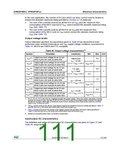
5.3.17
NRST pin characteristics
The NRST pin input driver uses CMOS technology. It is connected to a permanent pull-up
resistor, R (see Table 47).
PU
Unless otherwise specified, the parameters given in Table 50 are derived from tests
performed under the ambient temperature and V supply voltage conditions summarized
DD
in Table 14.
DocID022152 Rev 4
113/185

 STMICROELECTRONICS [ ST ]