Electrical characteristics
STM32F405xx, STM32F407xx
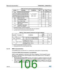
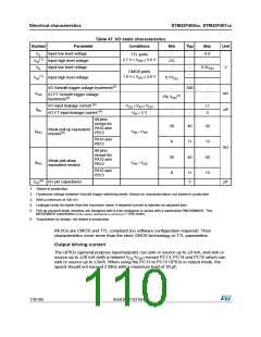
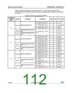
Table 47. I/O static characteristics
Conditions
Symbol
Parameter
Min
Typ
Max
Unit
VIL
Input low level voltage
Input high level voltage
Input low level voltage
-
2.0
-
-
0.8
TTL ports
(1)
2.7 V ≤ VDD ≤ 3.6 V
VIH
-
-
VIL
-
0.3VDD
V
CMOS ports
-
-
-
-
-
(1)
1.8 V ≤ VDD ≤ 3.6 V
VIH
Input high level voltage
0.7VDD
-
I/O Schmitt trigger voltage hysteresis(2)
200
Vhys
mV
µA
IO FT Schmitt trigger voltage
hysteresis(2)
(3)
5% VDD
-
-
I/O input leakage current (4)
VSS ≤ VIN ≤ VDD
VIN = 5 V
-
-
-
-
1
3
Ilkg
I/O FT input leakage current (4)
All pins
except for
PA10 and
resistor(5)
PB12
30
8
40
11
40
50
15
50
15
Weak pull-up equivalent
RPU
VIN = VSS
PA10 and
PB12
kΩ
All pins
except for
PA10 and
PB12
30
8
Weak pull-down
equivalent resistor
RPD
VIN = VDD
PA10 and
PB12
11
5
(6)
CIO
I/O pin capacitance
pF
1. Tested in production.
2. Hysteresis voltage between Schmitt trigger switching levels. Based on characterization, not tested in production.
3. With a minimum of 100 mV.
4. Leakage could be higher than the maximum value, if negative current is injected on adjacent pins.
5. Pull-up and pull-down resistors are designed with a true resistance in series with a switchable PMOS/NMOS. This
MOS/NMOS contribution to the series resistance is minimum (~10% order).
6. Guaranteed by design, not tested in production.
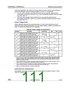
All I/Os are CMOS and TTL compliant (no software configuration required). Their
characteristics cover more than the strict CMOS-technology or TTL parameters.
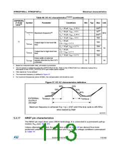
Output driving current
The GPIOs (general purpose input/outputs) can sink or source up to 8 mA, and sink or
source up to 20 mA (with a relaxed V /V ) except PC13, PC14 and PC15 which can
OL OH
sink or source up to 3mA. When using the PC13 to PC15 GPIOs in output mode, the
speed should not exceed 2 MHz with a maximum load of 30 pF.
110/185
DocID022152 Rev 4

 STMICROELECTRONICS [ ST ]