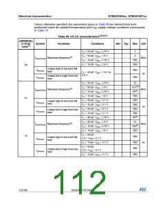
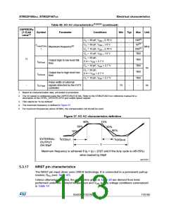
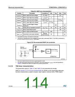
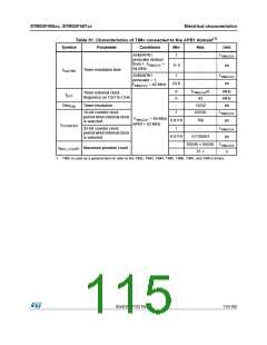
Electrical characteristics
STM32F405xx, STM32F407xx
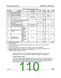
Unless otherwise specified, the parameters given in Table 49 are derived from tests
performed under the ambient temperature and V supply voltage conditions summarized
DD
in Table 14.
(1)(2)(3)
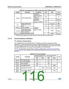
Table 49. I/O AC characteristics
OSPEEDRy
[1:0] bit
Symbol
Parameter
Conditions
Min
Typ
Max Unit
value(1)
CL = 50 pF, VDD > 2.70 V
CL = 50 pF, VDD > 1.8 V
CL = 10 pF, VDD > 2.70 V
CL = 10 pF, VDD > 1.8 V
-
-
-
-
-
-
-
-
2
2
fmax(IO)out Maximum frequency(4)
MHz
TBD
TBD
00
Output high to low level fall
tf(IO)out
time
-
-
-
-
TBD
ns
CL = 50 pF, VDD = 1.8 V to
3.6 V
Output low to high level rise
tr(IO)out
time
TBD
CL = 50 pF, VDD > 2.70 V
CL = 50 pF, VDD > 1.8 V
CL = 10 pF, VDD > 2.70 V
CL = 10 pF, VDD > 1.8 V
CL = 50 pF, VDD < 2.7 V
CL = 10 pF, VDD > 2.7 V
CL = 50 pF, VDD < 2.7 V
CL = 10 pF, VDD > 2.7 V
CL = 40 pF, VDD > 2.70 V
CL = 40 pF, VDD > 1.8 V
CL = 10 pF, VDD > 2.70 V
CL = 10 pF, VDD > 1.8 V
-
-
-
-
-
-
-
-
-
-
-
-
-
-
-
-
-
-
-
-
-
-
-
-
25
12.5(5)
MHz
fmax(IO)out Maximum frequency(4)
50(5)
TBD
TBD
01
Output high to low level fall
tf(IO)out
time
TBD
ns
TBD
Output low to high level rise
tr(IO)out
time
TBD
50(5)
25
fmax(IO)out Maximum frequency(4)
MHz
100(5)
TBD
TBD
CL = 50 pF,
10
-
-
-
-
-
-
-
-
Output high to low level fall
2.4 < VDD < 2.7 V
tf(IO)out
time
CL = 10 pF, VDD > 2.7 V
TBD
TBD
TBD
ns
CL = 50 pF,
Output low to high level rise
2.4 < VDD < 2.7 V
tr(IO)out
time
CL = 10 pF, VDD > 2.7 V
112/185
DocID022152 Rev 4

 STMICROELECTRONICS [ ST ]