Electrical characteristics
STM32F405xx, STM32F407xx
(1)
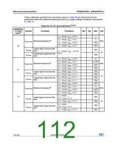
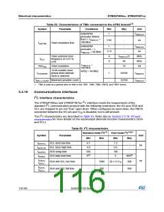
Table 52. Characteristics of TIMx connected to the APB2 domain
Symbol
Parameter
Conditions
Min
Max
Unit
AHB/APB2
1
-
tTIMxCLK
prescaler distinct
from 1, fTIMxCLK
168 MHz
=
5.95
-
ns
tres(TIM)
Timer resolution time
AHB/APB2
prescaler = 1,
fTIMxCLK = 84 MHz
1
11.9
0
-
tTIMxCLK
ns
-
fTIMxCLK/2
84
Timer external clock
frequency on CH1 to
CH4
MHz
MHz
bit
fEXT
0
fTIMxCLK
=
ResTIM
Timer resolution
-
16
168 MHz
16-bit counter clock
tCOUNTER period when internal
clock is selected
APB2 = 84 MHz
1
-
65536
32768
tTIMxCLK
tTIMxCLK
tMAX_COUNT Maximum possible count
1. TIMx is used as a general term to refer to the TIM1, TIM8, TIM9, TIM10, and TIM11 timers.
5.3.19
Communications interfaces
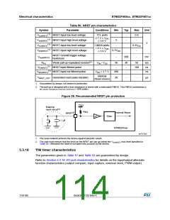
I2C interface characteristics
2
I
The STM32F405xx and STM32F407xx C interface meets the requirements of the
2
standard I C communication protocol with the following restrictions: the I/O pins SDA and
SCL are mapped to are not “true” open-drain. When configured as open-drain, the PMOS
connected between the I/O pin and V is disabled, but is still present.
DD
2
The I C characteristics are described in Table 53. Refer also to Section 5.3.16: I/O port
for more details on the input/output alternate function characteristics (SDA
characteristics
and SCL)
.
2
Table 53. I C characteristics
Standard mode I2C(1)
Fast mode I2C(1)(2)
Symbol
Parameter
Unit
Min
Max
Min
Max
tw(SCLL)
tw(SCLH)
tsu(SDA)
th(SDA)
SCL clock low time
SCL clock high time
SDA setup time
4.7
4.0
-
-
-
-
1.3
0.6
100
0
-
µs
-
250
0(3)
-
SDA data hold time
900(4)
tr(SDA)
tr(SCL)
ns
SDA and SCL rise time
SDA and SCL fall time
-
-
1000
300
20 + 0.1Cb
-
300
300
tf(SDA)
tf(SCL)
116/185
DocID022152 Rev 4

 STMICROELECTRONICS [ ST ]