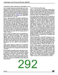
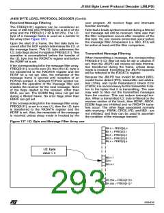
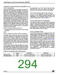
J1850 Byte Level Protocol Decoder (JBLPD)
J1850 BYTE LEVEL PROTOCOL DECODER (Cont’d)
10.9.4 Peripheral Functional Modes
tion when the JBLPD is not used, even if the de-
coder is able to follow the bus traffic. So, at any
time the JBLPD is enabled, it is immediately syn-
chronized with the J1850 bus.
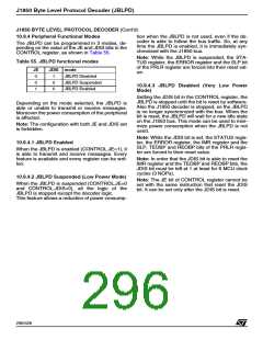
The JBLPD can be programmed in 3 modes, de-
pending on the value of the JE and JDIS bits in the
CONTROL register, as shown in Table 55.
Note: While the JBLPD is suspended, the STA-
TUS register, the ERROR register and the SLP bit
of the PRLR register are forced into their reset val-
ue.
Table 55. JBLPD functional modes
JE
0
JDIS mode
1
0
0
JBLPD Disabled
0
JBLPD Suspended
JBLPD Enabled
10.9.4.3 JBLPD Disabled (Very Low Power
Mode)
1
Setting the JDIS bit in the CONTROL register, the
JBLPD is stopped until the bit is reset by software.
Also the J1850 decoder is stopped, so the JBLPD
is no longer synchronized with the bus. When the
bit is reset, the JBLPD will wait for a new idle state
on the J1850 bus. This mode can be used to mini-
mize power consumption when the JBLPD is not
used.
Depending on the mode selected, the JBLPD is
able or unable to transmit or receive messages.
Moreover the power consumption of the peripheral
is affected.
Note: The configuration with both JE and JDIS set
is forbidden.
Note: While the JDIS bit is set, the STATUS regis-
ter, the ERROR register, the IMR register and the
SLP, TEOBP and REOBP bits of the PRLR regis-
ter are forced to their reset value.
10.9.4.1 JBLPD Enabled
When the JBLPD is enabled (CONTROL.JE=1), it
is able to transmit and receive messages. Every
feature is available and every register can be writ-
ten.
Note: In order that the JDIS bit is able to reset the
IMR register and the TEOBP and REOBP bits, the
JDIS bit must be left at 1 at least for 6 MCU clock
cycles (3 NOPs).
10.9.4.2 JBLPD Suspended (Low Power Mode)
Note: The JE bit of CONTROL register cannot be
set with the same instruction that reset the JDIS
bit. It can be set only after the JDIS bit is reset.
When the JBLPD is suspended (CONTROL.JE=0
and CONTROL.JDIS=0), all the logic of the
JBLPD is stopped except the decoder logic.
This feature allows a reduction of power consump-
296/426
9

 STMICROELECTRONICS [ ST ]