J1850 Byte Level Protocol Decoder (JBLPD)
J1850 BYTE LEVEL PROTOCOL DECODER (Cont’d)
Received Message Filtering
user program. All receiver flags and interrupts
function normally.
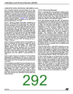
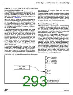
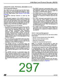
The FREG[0:31] registers can be considered an
array of 256 bits (the FREG[0].0 bit is bit 0 of the
array and the FREG[31].7 bit is bit 255). The I.D.
byte of a message frame is used as a pointer to
the array (See Figure 137).
Note that a break symbol received during a filtered
out message will still be received. Note also that
the filter comparison occurs after reception of the
first byte. So, any receive errors that occur before
the message filter comparison (i.e. IBD, IFD) will
be active at least until the filter comparison.
Upon the start of a frame, the first data byte re-
ceived after the SOF symbol determines the I.D. of
the message frame. This I.D. byte addresses the
I.D. byte flags stored in registers FREG[0:31]. This
operation is accomplished before the transfer of
the I.D. byte into the RXDATA register and before
the RDRF bit is set.
Transmitted Message Filtering
When transmitting a message, the corresponding
FREG[0:31] I.D. filter bit may be set or cleared. If
set, then the JBLPD will receive all data informa-
tion transferred during the frame, unless sleep
mode is invoked. Everything the JBLPD transmits
will be reflected in the RXDATA register.
If the corresponding bit in the message filter array,
FREG[0:31], is set to zero (0), then the I.D. byte is
not transferred to the RXDATA register and the
RDRF bit is not set. Also, the remainder of the
message frame is ignored until reception of an
EOFmin symbol. A received EOFmin symbol ter-
minates the operation of the message filter and
enables the receiver for the next message. None
of the flags related to the receiver, other than
IDLE, are set. The EODM flag does not get set
during a filtered frame. No error flags other than
RBRK can get set.
Because the JBLPD has invalid bit detect (IBD),
invalid frame detect (IFD), transmitter lost arbitra-
tion (TRA), and Cyclic Redundancy Check Error
(CRCE) it is not necessary for the transmitter to lis-
ten to the bytes that it is transmitting. The user
may wish to filter out the transmitted messages
from the receiver. This can reduce interrupt bur-
den. When a transmitted I.D. byte is filtered by the
receiver section of the block, then RDRF, RDOF,
EODM flags are inhibited and no RXDATA trans-
fers occur. The other flags associated normally
with receiving - RBRK, CRCE, IFD, and IBD - are
not inhibited, and they can be used to ascertain
the condition of the message transmit.
If the corresponding bit in the message filter array,
FREG[0:31], is set to a one (1), then the I.D. byte
is transferred to the RXDATA register and the
RDRF is set. Also, the remainder of the message
is received unless sleep mode is invoked by the
Figure 137. I.D. Byte and Message Filter Array use
Bit 0 = FREG[0].0
Bit 1 = FREG[0].1
Bit 2 = FREG[0].2
Bit 3 = FREG[0].3
Bit 4 = FREG[0].4
I.D. byte
value = n
Bit n-1
Bit n
Bit n+1
Bit 254 = FREG[31].6
Bit 255 = FREG[31].7
293/426
9

 STMICROELECTRONICS [ ST ]