J1850 Byte Level Protocol Decoder (JBLPD)
J1850 BYTE LEVEL PROTOCOL DECODER (Cont’d)
10.9.3.4 Sleep Mode
ing the TRDY, TLA, TTO, TDUF, TRA, IBD, IFD,
and CRCE bits to be set if required. This mode al-
lows the user to not have to listen while talking.
Sleep mode allows the user program to ignore the
remainder of a message. Normally, the user pro-
gram can recognise if the message is of interest
from the header bytes at the beginning of the mes-
sage. If the user program is not interested in the
message it simply writes the SLP bit in the PRLR
register. This causes all additional data on the bus
to be ignored until an EOF minimum occurs. No
additional flags (but not the EOFM flag) and, there-
fore, interrupts are generated for the remainder of
the message. The single exception to this is a re-
ceived break symbol while in sleep mode. Break
symbols always take precedence and will set the
RBRK bit in the ERROR register and generate an
interrupt if the ERR_M bit in IMR is set. Sleep
mode and the SLP bit gets cleared on reception of
an EOF or Break symbol.
10.9.3.5 Normalization Bit symbol selection
The form of the NB0/NB1 symbol changes de-
pending on the industry standard followed. A bit
(NBSYMS) in the OPTIONS register selects the
symbol timings used. Refer to Table 54.
10.9.3.6 VPWI input line management
The JBLPD is able to work with J1850 transceiver
chips that have both inverted and not inverted RX
signal. A dedicated bit (INPOL) of the OPTIONS
register must be programmed with the correct val-
ue depending on the polarity of the VPWI input
with respect to the J1850 bus line. Refer to the IN-
POL bit description for more details.
Writes to the SLP bit will be ignored if:
1) A valid EOFM symbol was the last valid symbol
detected,
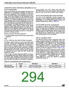
10.9.3.7 Loopback mode
AND
The JBLPD is able to work in loopback mode. This
mode, enabled setting the LOOPB bit of the OP-
TIONS register, internally connects the output sig-
nal (VPWO) of the JBLPD to the input (VPWI)
without polarity inversion. The external VPWO pin
of the MCU is forced in its passive state and the
external VPWI pin is ignored (Refer to Figure 138).
2) The J1850 bus line (after the filter) is passive.
Therefore, sleep mode can only be invoked after
the SOF symbol and subsequent data has been
received, but before a valid EOF is detected. If
sleep mode is invoked within this time window,
then any queued IFR transmit is aborted. If a MSG
type is queued and sleep mode is invoked, then
the MSG type will remain queued and an attempt
to transmit will occur after the EOF period has
elapsed as usual.
Note: When the LOOPB bit is set or reset, edges
could be detected by the J1850 decoder on the in-
ternal VPWI line. These edges could be managed
by the JBLPD as J1850 protocol errors. It is sug-
gested to enable/disable LOOPB when the JBLPD
If SLP mode is invoked while the JBLPD is current-
ly transmitting, then the JBLPD effectively inhibits
the RDRF, RDT, EODM, & RDOF flags from being
set, and disallows RXDATA transfers. But, it other-
wise functions normally as a transmitter, still allow-
is
suspended
(CONTROL.JE=0,
CON-
TROL.JDIS=0) or when the JBLPD is disabled
(CONTROL.JDIS=1).
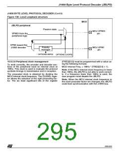
Table 54. Normalization Bit configurations
Symbol
NB0
NBSYMS=0
active Tv2 (active long)
active Tv1 (active short)
NBSYMS=1
IFR with CRC
active Tv1 (active short)
active Tv2 (active long)
IFR without CRC
NB1
294/426
9

 STMICROELECTRONICS [ ST ]