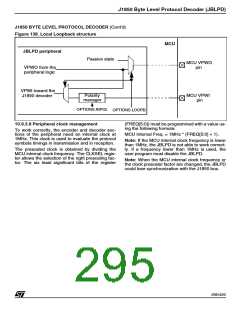
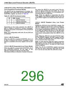
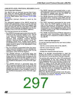
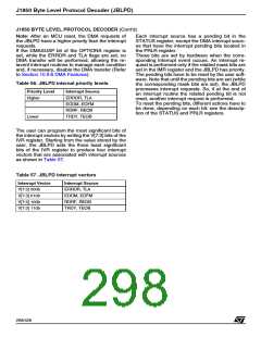
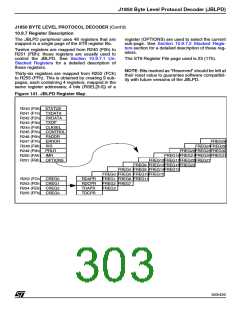
J1850 Byte Level Protocol Decoder (JBLPD)
J1850 BYTE LEVEL PROTOCOL DECODER (Cont’d)
10.9.6 DMA Features
(odd address). They are pointed to by the DMA
Transaction Counter Pointer Register (RDCPR
register in receiving, TDCPR register in transmit-
ting) located in the JBLPD register page.
The JBLPD can use the ST9 on-chip Direct Mem-
ory Access (DMA) channels to provide high-speed
data transactions between the JBLPD and contig-
uous locations of Register File and Memory. The
transactions can occur from and toward the
JBLPD. The maximum number of transactions that
each DMA channel can perform is 222 with Regis-
ter File or 65536 with Memory. Control of the DMA
features is performed using registers located in the
JBLPD register page (IVR, PRLR, IMR, RDAPR,
RDCPR, TDAPR, TDCPR).
To select DMA transactions with the Register File,
the control bits RDCPR.RF/MEM in receiving
mode or TDCPR.RF/MEM in transmitting mode
must be set.
The transaction Counter Register must be initial-
ized with the number of DMA transfers to perform
and it will be decremented after each transaction.
The DMA Address Register must be initialized with
the starting address of the DMA table in the Regis-
ter File, and it is incremented after each transac-
tion. These two registers must be located between
addresses 00h and DFh of the Register File.
The priority level of the DMA features of the
JBLPD with respect to the other ST9 peripherals
and the CPU is the same as programmed in the
PRLR register for the interrupt sources. In the in-
ternal priority level order of the JBLPD, depending
on the value of the DMASUSP bit in the OPTIONS
register, the DMA may or may not have a higher
priority than the interrupt sources.
When the DMA occurs between JBLPD and Reg-
ister File, the TDAPR register (in transmission)
and the RDAPR register (in reception) are not
used.
Refer to the Interrupt and DMA chapters of the da-
tasheet for details on priority levels.
10.9.6.2 DMA between JBLPD and Memory
Space
The DMA features are enabled by setting the ap-
propriate enabling bits (RXD_M, TXD_M) in the
IMR register. It is also possible to select the direc-
tion of the DMA transactions.
If the DMA transaction is made between the
JBLPD and Memory, a register pair is required to
hold the DMA Address and another register pair to
hold the DMA Transaction counter. These two
pairs of registers must be located in the Register
File. The DMA Address pair is pointed to by the
DMA Address Pointer Registers (RDAPR register
in reception, TDAPR register in transmission) lo-
cated in the JBLPD register page; the DMA Trans-
action Counter pair is pointed to by the DMA
Transaction Counter Pointer Registers (RDCPR
register in reception, TDCPR register in transmis-
sion) located in the JBLPD register page.
Once the DMA table is completed (the transaction
counter reaches 0 value), an interrupt request to
the CPU is generated if the related mask bit is set
(RDRF_M bit in reception, TRDY_M bit in trans-
mission). This kind of interrupt is called “End Of
Block”. The peripheral sends two different “End Of
Block” interrupts depending on the direction of the
DMA (Receiving End Of Block (REOB) - Transmit-
ting End Of Block (TEOB)). These interrupt sourc-
es have dedicated interrupt pending bits in the
PRLR register (REOBP, TEOBP) and they are
mapped to the same interrupt vectors: “Receive
Data Register Full (RDRF)” and “Transmit Ready
(TRDY)” respectively. The same correspondence
exists for the internal priority between interrupts
and interrupt vectors.
To select DMA transactions with Memory Space,
the control bits RDCPR.RF/MEM in receiving
mode or TDCPR.RF/MEM in transmitting mode
must be reset.
The Transaction Counter register pair must be ini-
tialized with the number of DMA transfers to per-
form and it will be decremented after each transac-
tion. The DMA Address register pair must be ini-
tialized with the starting address of the DMA table
in Memory Space, and it is incremented after each
transaction. These two register pairs must be lo-
cated between addresses 00h and DFh of the
Register File.
10.9.6.1 DMA between JBLPD and Register File
If the DMA transaction is made between the
JBLPD and the Register File, one register is re-
quired to hold the DMA Address and one to hold
the DMA transaction counter. These two registers
must be located in the Register File: the DMA Ad-
dress Register in an even addressed register, the
DMA Transaction Counter in the following register
299/426
9

 STMICROELECTRONICS [ ST ]