J1850 Byte Level Protocol Decoder (JBLPD)
J1850 BYTE LEVEL PROTOCOL DECODER (Cont’d)
Use of symbol and bit synchronization is an inte-
gral part of the J1850 bus scheme. Therefore, tight
coupling of the encoder and decoder functions is
required to maintain synchronization during trans-
mits. Transmitted symbols and bits are initiated by
the encoder and are timed through the decoder to
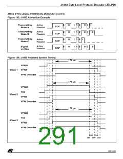
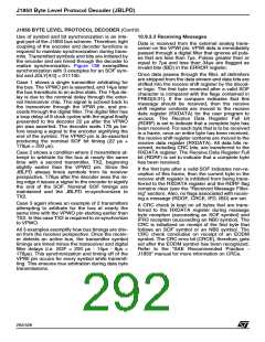
realize synchronization. Figure 136 exemplifies
synchronization with 3 examples for an SOF sym-
bol and JDLY[4:0] = 01110b.
10.9.3.3 Receiving Messages
Data is received from the external analog trans-
ceiver on the VPWI pin. VPWI data is immediately
passed through a digital filter that ignores all puls-
es that are less than 7µs. Pulses greater than or
equal to 7µs and less than 34µs are flagged as
invalid bits (IBD) in the ERROR register.
Once data passes through the filter, all delimiters
are stripped from the data stream and data bits are
shifted into the receive shift register by the decod-
er logic. The first byte received after a valid SOF
character is compared with the flags contained in
FREG[0:31]. If the compare indicates that this
message should be received, then the receive
shift register contents are moved to the receive
data register (RXDATA) for the user program to
access. The Receive Data Register Full bit
(RDRF) is set to indicate that a complete byte has
been received. For each byte that is to be received
in a frame, once an entire byte has been received,
the receive shift register contents are moved to the
receive data register (RXDATA). All data bits re-
ceived, including CRC bits, are transferred to the
RXDATA register. The Receive Data Register Full
bit (RDRF) is set to indicate that a complete byte
has been received.
Case 1 shows a single transmitter arbitrating for
the bus. The VPWO pin is asserted, and 14µs later
the bus transitions to an active state. The 14µs de-
lay is due to the nominal delay through the exter-
nal transceiver chip. The signal is echoed back to
the transceiver through the VPWI pin, and pro-
ceeds through the digital filter. The digital filter has
a loop delay of 8 clock cycles with the signal finally
presented to the decoder 22 µs after the VPWO
pin was asserted. The decoder waits 178 µs be-
fore issuing a signal to the encoder signifying the
end of the symbol. The VPWO pin is de-asserted
producing the nominal SOF bit timing (22 µs +
178µs = 200 µs).
Case 2 shows a condition where 2 transmitters at-
tempt to arbitrate for the bus at nearly the same
time with a second transmitter, TX2, beginning
slightly earlier than the VPWO pin. Since the
JBLPD always times symbols from its receiver
perspective, 178µs after the decoder sees the ris-
ing edge it issues a signal to the encoder to signify
the end of the SOF. Nominal SOF timings are
maintained and the JBLPD re-synchronizes to
TX2.
If the first byte after a valid SOF indicates non-re-
ception of this frame, then the current byte in the
receive shift register is inhibited from being trans-
ferred to the RXDATA register and the RDRF flag
remains clear (see the “Received Message Filter-
ing” section). Also, no flags associated with receiv-
ing a message (RDOF, CRCE, IFD, IBD) are set.
Case 3 again shows an example of 2 transmitters
attempting to arbitrate for the bus at nearly the
same time with the VPWO pin starting earlier than
TX2. In this case TX2 is required to re-synchronize
to VPWO.
A CRC check is kept on all bytes that are trans-
ferred to the RXDATA register during message
byte reception (succeeding an SOF symbol) and
IFR3 reception (succeeding an NB0 symbol). The
CRC is initialized on receipt of the first byte that
follows an SOF symbol or an NB0 symbol. The
CRC check concludes on receipt of an EODM
symbol. The CRC error bit (CRCE), therefore, gets
set after the EODM symbol has been recognized.
Refer to the “SAE Recommended Practice -
J1850” manual for more information on CRCs.
All 3 examples exemplify how bus timings are driv-
en from the receiver perspective. Once the receiv-
er detects an active bus, the transmitter symbol
timings are timed minus the transceiver and digital
filter delays (i.e. SOF = 200 µs - 14µs - 8µs =
178µs). This synchronization and timing off of the
VPWI pin occurs for every symbol while transmit-
ting. This ensures true arbitration during data byte
transmissions.
292/426
9

 STMICROELECTRONICS [ ST ]