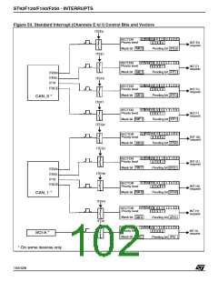
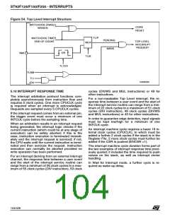
ST92F124/F150/F250 - INTERRUPTS
INTERRUPT REGISTERS (Cont’d)
EXTERNAL INTERRUPT PENDING REGISTER
(EIPR)
Bit 3 = IMB1: INTB1 Interrupt Mask
Bit 2 = IMB0: INTB0 Interrupt Mask
Bit 1 = IMA1: INTA1 Interrupt Mask
Bit 0 = IMA0: INTA0 Interrupt Mask
R243 - Read/Write
Register Page: 0
Reset value: 0000 0000 (00h)
These bits are set and cleared by software.
0: Interrupt masked
7
0
1: Interrupt not masked (an interrupt is generated if
the IPxx and IEN bits = 1)
IPD1 IPD0 IPC1 IPC0 IPB1 IPB0 IPA1 IPA0
Bit 7 = IPD1: INTD1 Interrupt Pending bit
Bit 6 = IPD0: INTD0 Interrupt Pending bit
Bit 5 = IPC1: INTC1 Interrupt Pending bit
Bit 4 = IPC0: INTC0 Interrupt Pending bit
Bit 3 = IPB1: INTB1 Interrupt Pending bit
Bit 2 = IPB0: INTB0 Interrupt Pending bit
Bit 1 = IPA1: INTA1 Interrupt Pending bit
Bit 0 = IPA0: INTA0 Interrupt Pending bit
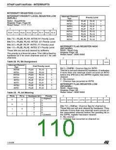
EXTERNAL INTERRUPT PRIORITY LEVEL
REGISTER (EIPLR)
R245 - Read/Write
Register Page: 0
Reset value: 1111 1111 (FFh)
7
0
PL2D PL1D PL2C PL1C PL2B PL1B PL2A PL1A
These bits are set by hardware on occurrence of a
trigger event (as specified in the EITR register)
and are cleared by hardware on interrupt acknowl-
edge. They can also be set by software to imple-
ment a software interrupt.
Bits 7:6 = PL2D, PL1D: INTD0, D1 Priority Level.
Bis 5:4 = PL2C, PL1C: INTC0, C1 Priority Level.
Bits 3:2 = PL2B, PL1B: INTB0, B1 Priority Level.
Bits 1:0 = PL2A, PL1A: INTA0, A1 Priority Level.
These bits are set and cleared by software.
0: No interrupt pending
1: Interrupt pending
The priority is a three-bit value. The LSB is fixed by
hardware at 0 for Channels A0, B0, C0 and D0 and
at 1 for Channels A1, B1, C1 and D1.
EXTERNAL INTERRUPT MASK-BIT REGISTER
(EIMR)
Hardware
R244 - Read/Write
PL2x PL1x
Priority
0 (Highest)
bit
Register Page: 0
Reset value: 0000 0000 (00h)
0
1
0
0
1
1
0
1
0
1
1
7
0
0
1
2
3
IMD1 IMD0 IMC1 IMC0 IMB1 IMB0 IMA1 IMA0
0
1
4
5
Bit 7 = IMD1: INTD1 Interrupt Mask
Bit 6 = IMD0: INTD0 Interrupt Mask
Bit 5 = IMC1: INTC1 Interrupt Mask
Bit 4 = IMC0: INTC0 Interrupt Mask
0
1
6
7 (Lowest)
106/426
9

 STMICROELECTRONICS [ ST ]