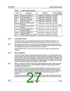
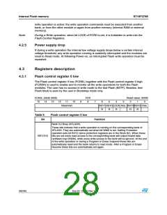
Internal Flash memory
ST10F276E
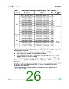
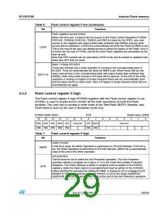
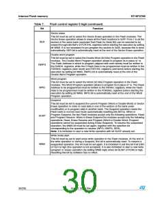
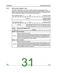
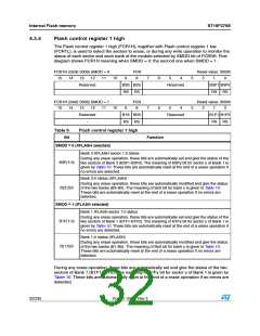
Table 7.
Bit
Flash control register 0 high (continued)
Function
Sector erase
This bit must be set to select the Sector Erase operation in the Flash modules. The
Sector Erase operation allows to erase all the Flash locations to 0xFF. From 1 to all the
sectors of the same bank (excluded Test-Flash for Bank B0) can be selected to be
erased through bits BxFy of FCR1H/L registers before starting the execution by setting
bit WMS. It is not necessary to pre-program the sectors to 0x00, because this is done
automatically. SER bit is automatically reset at the end of the Sector Erase operation.
SER
DWPG
WPG
Double word program
This bit must be set to select the Double Word (64 bits) Program operation in the Flash
modules. The Double Word Program operation allows to program 0s in place of 1s.
The Flash Address in which to program (aligned with even words) must be written in
the FARH/L registers, while the 2 Flash Data to be programmed must be written in the
FDR0H/L registers (even word) and FDR1H/L registers (odd word) before starting the
execution by setting bit WMS. DWPG bit is automatically reset at the end of the
Double Word Program operation.
Word program
This bit must be set to select the Word (32 bits) Program operation in the Flash
modules. The Word Program operation allows to program 0s in place of 1s. The Flash
Address to be programmed must be written in the FARH/L registers, while the Flash
Data to be programmed must be written in the FDR0H/L registers before starting the
execution by setting bit WMS. WPG bit is automatically reset at the end of the Word
Program operation.
Suspend
This bit must be set to suspend the current Program (Word or Double Word) or Sector
Erase operation in order to read data in one of the sectors of the bank under
modification or to program data in another bank. The Suspend operation resets the
Flash bank to normal read mode (automatically resetting bits BSYx). When in
Program Suspend, the two Flash modules accept only the following operations: Read
and Program Resume. When in Erase Suspend the modules accept only the following
operations: Read, Erase Resume and Program (Word or Double Word; Program
operations cannot be suspended during Erase Suspend). To resume the suspended
operation, the WMS bit must be set again, together with the selection bit
corresponding to the operation to resume (WPG, DWPG, SER).
SUSP
Note: It is forbidden to start a new Write operation with bit SUSP already set.
Write mode start
This bit must be set to start every write operation in the Flash modules. At the end of
the write operation or during a Suspend, this bit is automatically reset. To resume a
suspended operation, this bit must be set again. It is forbidden to set this bit if bit ERR
of FER is high (the operation is not accepted). It is also forbidden to start a new write
(program or erase) operation (by setting WMS high) when bit SUSP of FCR0 is high.
Resetting this bit by software has no effect.
WMS
30/235
Doc ID 12303 Rev 3

 STMICROELECTRONICS [ ST ]