ST10F276E
Pin data
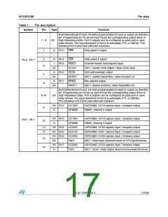
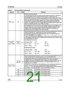
Table 1.
Symbol
Pin description
Pin
Type
Function
8-bit bidirectional I/O port, bit-wise programmable for input or output via direction
bit. Programming an I/O pin as input forces the corresponding output driver to
high impedance state. Port 6 outputs can be configured as push-pull or open
drain drivers. The input threshold of Port 6 is selectable (TTL or CMOS). The
following Port 6 pins have alternate functions:
1 - 8
I/O
1
...
5
O
P6.0
CS0
Chip select 0 output
... ...
...
...
O
I
P6.4
CS4
Chip select 4 output
P6.0 - P6.7
P6.5
P6.6
P6.7
HOLD
SCLK1
HLDA
MTSR1
BREQ
MRST1
External master hold request input
SSC1: master clock output / slave clock input
Hold acknowledge output
6
7
8
I/O
O
I/O
O
SSC1: master-transmitter / slave-receiver O/I
Bus request output
I/O
SSC1: master-receiver / slave-transmitter I/O
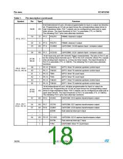
8-bit bidirectional I/O port, bit-wise programmable for input or output via direction
bit. Programming an I/O pin as input forces the corresponding output driver to
9-16
I/O high impedance state. Port 8 outputs can be configured as push-pull or open
drain drivers. The input threshold of Port 8 is selectable (TTL or CMOS).
The following Port 8 pins have alternate functions:
I/O P8.0
O
CC16IO
XPWM0
...
CAPCOM2: CC16 capture input / compare output
PWM1: channel 0 output
9
...
... ...
I/O P8.3
O
...
CC19IO
XPWM0
CC20IO
CC21IO
CC22IO
RxD1
CAPCOM2: CC19 capture input / compare output
PWM1: channel 3 output
P8.0 - P8.7
12
13
14
I/O P8.4
I/O P8.5
I/O P8.6
I/O
CAPCOM2: CC20 capture input / compare output
CAPCOM2: CC21 capture input / compare output
CAPCOM2: CC22 capture input / compare output
ASC1: Data input (Asynchronous) or I/O (Synchronous)
CAPCOM2: CC23 capture input / compare output
ASC1: Clock / Data output (Asynchronous/Synchronous)
15
16
I/O P8.7
O
CC23IO
TxD1
Doc ID 12303 Rev 3
17/235

 STMICROELECTRONICS [ ST ]