Electrical characteristics
ST10F276E
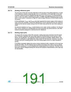
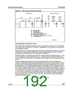
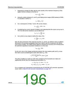
Figure 47. A/D converter input pins scheme
%XTERNAL CIRCUIT
)NTERNAL CIRCUIT SCHEME
6
$$
#HANNEL
SELECTION
3AMPLING
3OURCE
&ILTER
#URRENT LIMITER
2
2
2
2
2
!$
3
&
,
37
#
6
#
#
#
3
!
&
0ꢀ
0ꢁ
2
2
#
2
2
2
#
#
3OURCE IMPEDANCE
&ILTER RESISTANCE
&ILTER CAPACITANCE
#URRENT LIMITER RESISTANCE
#HANNEL SELECTION SWITCH IMPEDANCE
3AMPLING SWITCH IMPEDANCE
3
&
&
,
37
!$
0
0IN CAPACITANCE ꢍTWO CONTRIBUTIONSꢗ # AND #
0ꢀ
3AMPLING CAPACITANCE
ꢏ
0ꢁ
3
'!0'2)ꢉꢉꢀꢁꢇ
Input leakage and external circuit
The series resistor utilized to limit the current to a pin (see RL in Figure 47), in combination
with a large source impedance, can lead to a degradation of A/D converter accuracy when
input leakage is present.
Data about maximum input leakage current at each pin is provided in Section 23: Electrical
characteristics. Input leakage is greatest at high operating temperatures and in general
decreases by one half for each 10°C decrease in temperature.
Considering that, for a 10-bit A/D converter one count is about 5mV (assuming VAREF = 5V),
an input leakage of 100nA acting though an RL = 50kΩ of external resistance leads to an
error of exactly one count (5mV); if the resistance were 100kΩ, the error would become two
counts.
Eventual additional leakage due to external clamping diodes must also be taken into
account in computing the total leakage affecting the A/D converter measurements. Another
contribution to the total leakage is represented by the charge sharing effects with the sam-
pling capacitance: CS being substantially a switched capacitance, with a frequency equal to
the conversion rate of a single channel (maximum when fixed channel continuous conver-
sion mode is selected), it can be seen as a resistive path to ground. For instance, assuming
a conversion rate of 250 kHz, with CS equal to 4pF, a resistance of 1MΩ is obtained (REQ
1 / fCCS, where fC represents the conversion rate at the considered channel). To minimize
the error induced by the voltage partitioning between this resistance (sampled voltage on
CS) and the sum of RS + RF + RL + RSW + RAD, the external circuit must be designed to
respect the following relation:
=
R
+ R + R + R
+ R
S
F
L
SW
------------------------------------------------------------------------------ --
LSB
AD
1
2
V
⋅
<
A
R
EQ
192/235
Doc ID 12303 Rev 3

 STMICROELECTRONICS [ ST ]