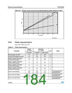
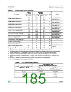
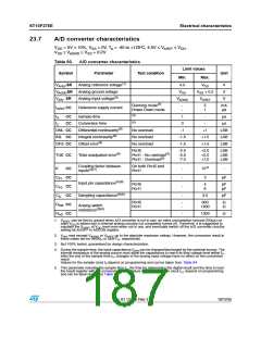
Electrical characteristics
ST10F276E
6. DNL, INL, OFS and TUE are tested at V
= 5.0V, V
= 0V, V = 5.0V. It is guaranteed by design
AGND DD
AREF
characterization for all other voltages within the defined voltage range.
“LSB” has a value of V /1024.
AREF
For Port5 channels, the specified TUE ( 2LSB) is also guaranteed with an overload condition (see IOV
specification) occurring on a maximum of 2 not selected analog input pins of Port5 and the absolute sum of
input overload currents on all Port5 analog input pins does not exceed 10 mA.
For Port1 channels, the specified TUE is guaranteed when no overload condition is applied to Port1 pins:
When an overload condition occurs on a maximum of 2 not selected analog input pins of Port1 and the
input positive overload current on all analog input pins does not exceed 10 mA (either dynamic or static
injection), the specified TUE is degraded ( 7LSB). To obtain the same accuracy, the negative injection
current on Port1 pins shall not exceed -1mA in case of both dynamic and static injection.
7. The coupling factor is measured on a channel while an overload condition occurs on the adjacent not
selected channels with the overload current within the different specified ranges (for both positive and
negative injection current).
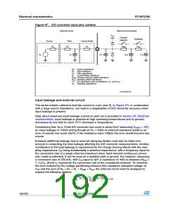
8. Refer to scheme shown in Figure 47
23.7.1
Conversion timing control
When a conversion starts, first the capacitances of the converter are loaded via the respec-
tive analog input pin to the current analog input voltage. The time to load the capacitances is
referred to as sample time. Next, the sampled voltage is converted in several successive
steps into a digital value, which corresponds to the 10-bit resolution of the ADC. During
these steps the internal capacitances are repeatedly charged and discharged via the VAREF
pin.
The current that must be drawn from the sources for sampling and changing charges
depends on the duration of each step because the capacitors must reach their final voltage
level within the given time, at least with a certain approximation. However, the maximum cur-
rent that a source can deliver depends on its internal resistance.
The time that the two different actions take during conversion (sampling and converting) can
be programmed within a certain range in the ST10F276E relative to the CPU clock. The
absolute time consumed by the different conversion steps is therefore independent from the
general speed of the controller. This allows adjusting the ST10F276E A/D converter to the
properties of the system:
Fast conversion can be achieved by programming the respective times to their absolute
possible minimum. This is preferable for scanning high frequency signals. However, the
internal resistance of analog source and analog supply must be sufficiently low.
High internal resistance can be achieved by programming the respective times to a higher
value or to the possible maximum. This is preferable when using analog sources and supply
with a high internal resistance in order to keep the current as low as possible. However, the
conversion rate in this case may be considerably lower.
The conversion times are programmed via the upper 4 bits of register ADCON. Bit fields
ADCTC and ADSTC define the basic conversion time and in particular the partition between
the sample phase and comparison phases. The table below lists the possible combinations.
The timings refer to the unit TCL, where fCPU = 1/2TCL. A complete conversion time
includes the conversion itself, the sample time and the time required to transfer the digital
value to the result register.
Table 94. A/D converter programming
ADCTC ADSTC
Sample
Comparison
TCL * 240
Extra
Total conversion
00
00
00
01
TCL * 120
TCL * 140
TCL * 28
TCL * 16
TCL * 388
TCL * 436
TCL * 280
188/235
Doc ID 12303 Rev 3

 STMICROELECTRONICS [ ST ]