ST10F276E
Electrical characteristics
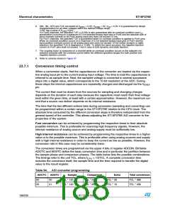
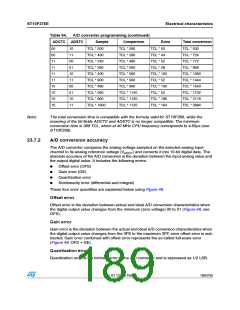
Table 94. A/D converter programming (continued)
ADCTC ADSTC Sample Comparison
TCL * 200 TCL * 280
Extra
Total conversion
00
10
11
00
01
10
11
00
01
10
11
TCL * 52
TCL * 44
TCL * 52
TCL * 28
TCL * 100
TCL * 52
TCL * 100
TCL * 52
TCL * 196
TCL * 164
TCL * 532
TCL * 724
TCL * 772
TCL * 868
TCL * 1060
TCL * 1444
TCL * 1540
TCL * 1732
TCL * 2116
TCL * 2884
00
11
11
11
11
10
10
10
10
TCL * 400
TCL * 240
TCL * 280
TCL * 400
TCL * 800
TCL * 480
TCL * 560
TCL * 800
TCL * 1600
TCL * 280
TCL * 480
TCL * 560
TCL * 560
TCL * 560
TCL * 960
TCL * 1120
TCL * 1120
TCL * 1120
Note:
The total conversion time is compatible with the formula valid for ST10F269, while the
meaning of the bit fields ADCTC and ADSTC is no longer compatible: The minimum
conversion time is 388 TCL, which at 40 MHz CPU frequency corresponds to 4.85μs (see
ST10F269).
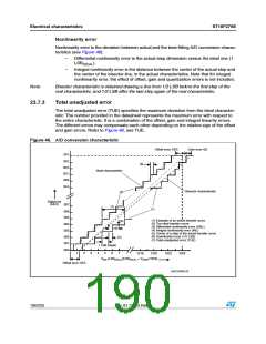
23.7.2
A/D conversion accuracy
The A/D converter compares the analog voltage sampled on the selected analog input
channel to its analog reference voltage (VAREF) and converts it into 10-bit digital data. The
absolute accuracy of the A/D conversion is the deviation between the input analog value and
the output digital value. It includes the following errors:
●
●
●
●
Offset error (OFS)
Gain error (GE)
Quantization error
Nonlinearity error (differential and integral)
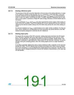
These four error quantities are explained below using Figure 46.
Offset error
Offset error is the deviation between actual and ideal A/D conversion characteristics when
the digital output value changes from the minimum (zero voltage) 00 to 01 (Figure 46, see
OFS).
Gain error
Gain error is the deviation between the actual and ideal A/D conversion characteristics when
the digital output value changes from the 3FE to the maximum 3FF, once offset error is sub-
tracted. Gain error combined with offset error represents the so-called full-scale error
(Figure 46, OFS + GE).
Quantization error
Quantization error is the intrinsic error of the A/D converter and is expressed as 1/2 LSB.
Doc ID 12303 Rev 3
189/235

 STMICROELECTRONICS [ ST ]