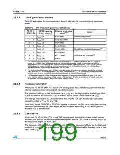
ST10F276E
Electrical characteristics
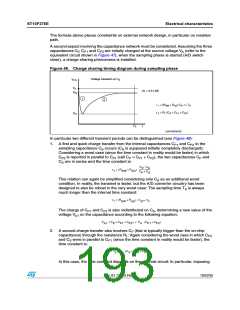
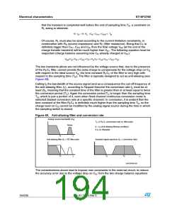
above, it is simple to derive the following relation between the ideal and real sampled volt-
age on CS:
V
C
+ C
+ C
F
A
P1
----------- = ------------------------------------------------------------
+ C + C + C
P2
V
C
A2
P1
P2
F
S
From this formula, in the worst case (when VA is maximum, that is for instance 5V), assum-
ing to accept a maximum error of half a count (~2.44mV), it is immediately evident that a
constraint is on CF value:
C
> 2048 C⋅
S
F
The next section provides an example of how to design the external network, based on
some reasonable values for the internal parameters and on a hypothesis on the characteris-
tics of the analog signal to be sampled.
23.7.6
Example of external network sizing
The following hypothesis is formulated in order to proceed with designing the external net-
work on A/D converter input pins:
–
–
–
–
–
–
–
–
–
–
–
Analog signal source bandwidth (f0):
Conversion rate (fC):
10 kHz
25 kHz
1µs
Sampling time (TS):
Pin input capacitance (CP1):
5pF
Pin input routing capacitance (CP2):
Sampling capacitance (CS):
1pF
4pF
Maximum input current injection (IINJ):
Maximum analog source voltage (VAM)
Analog source impedance (RS):
Channel switch resistance (RSW):
Sampling switch resistance (RAD):
3mA
12V
:
100Ω
500Ω
200Ω
Doc ID 12303 Rev 3
195/235

 STMICROELECTRONICS [ ST ]