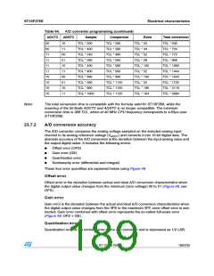
ST10F276E
Electrical characteristics
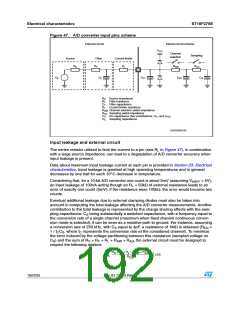
The formula above places constraints on external network design, in particular on resistive
path.
A second aspect involving the capacitance network must be considered. Assuming the three
capacitances CF, CP1 and CP2 are initially charged at the source voltage VA (refer to the
equivalent circuit shown in Figure 47), when the sampling phase is started (A/D switch
close), a charge sharing phenomena is installed.
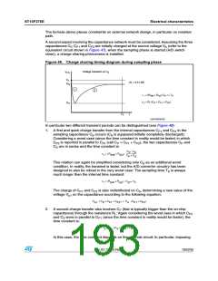
Figure 48. Charge sharing timing diagram during sampling phase
6OLTAGE TRANSIENT ON #
6
3
#3
6
!
'6 ꢘꢀꢉꢌꢃ ,3"ꢀ
6
!ꢁ
ꢀ
ꢁ
W
W
ꢘ ꢍ2
ꢑ 2 ꢏ # ꢘꢘ 4
37 !$ 3 3
ꢀ
ꢁ
ꢓ 2 ꢍ# ꢑ # ꢑ # ꢏ
0ꢁ
6
,
3
0ꢀ
!ꢀ
4
T
3
'!0'2)ꢉꢉꢀꢁꢃ
In particular two different transient periods can be distinguished (see Figure 48):
1. A first and quick charge transfer from the internal capacitances CP1 and CP2 to the
sampling capacitance CS occurs (CS is supposed initially completely discharged):
Considering a worst case (since the time constant in reality would be faster) in which
C
P2 is reported in parallel to CP1 (call CP = CP1 + CP2), the two capacitances CP and
CS are in series and the time constant is:
C
⋅ C
S
P
-----------------------
) ⋅
AD
τ
= (R
+ R
1
SW
C
+ C
P
S
This relation can again be simplified considering only CS as an additional worst
condition. In reality, the transient is faster, but the A/D converter circuitry has been
designed to also be robust in the very worst case: The sampling time TS is always
much longer than the internal time constant:
τ
< (R
+ R
) ⋅ C
<< TS
AD S
1
SW
The charge of CP1 and CP2 is also redistributed on CS, determining a new value of the
voltage VA1 on the capacitance according to the following equation:
V
⋅ (C + C
+ C ) = V ⋅ (C
P2
+ C
)
P2
A1
S
P1
A
P1
2. A second charge transfer also involves CF (that is typically bigger than the on-chip
capacitance) through the resistance RL: Again considering the worst case in which CP2
and CS were in parallel to CP1 (since the time constant in reality would be faster), the
time constant is:
τ
< R ⋅ (C + C
+ C
)
P2
2
L
S
P1
In this case, the time constant depends on the external circuit: In particular, imposing
Doc ID 12303 Rev 3
193/235

 STMICROELECTRONICS [ ST ]