Electrical characteristics
ST10F276E
that the transient is completed well before the end of sampling time TS, a constraint on
RL sizing is obtained:
10 ⋅ τ = 10 ⋅ R ⋅ (C + C
+ C ) ≤
P2
T
2
L
S
P1
S
Of course, RL must also be sized according to the current limitation constraints, in
combination with RS (source impedance) and RF (filter resistance). Being that CF is
definitely bigger than CP1, CP2 and CS, then the final voltage VA2 (at the end of the
charge transfer transient) will be much higher than VA1. The following equation must be
respected (charge balance assuming now CS already charged at VA1):
V
(⋅C +C
+C
+C ) =V ⋅C + V (⋅C
A1 P1
+C
+C )
S
A2
S
P1
P2
F
A
F
P2
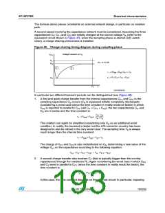
The two transients above are not influenced by the voltage source that, due to the presence
of the RFCF filter, cannot provide the extra charge to compensate for the voltage drop on CS
with respect to the ideal source VA; the time constant RFCF of the filter is very high with
respect to the sampling time (TS). The filter is typically designed to act as anti-aliasing (see
Figure 49).
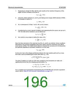
Calling f0 the bandwidth of the source signal (and as a consequence the cut-off frequency of
the anti-aliasing filter, fF), according to Nyquist theorem the conversion rate fC must be at
least 2f0, meaning that the constant time of the filter is greater than or at least equal to twice
the conversion period (TC). Again the conversion period TC is longer than the sampling time
TS, which is just a portion of it, even when fixed channel continuous conversion mode is
selected (fastest conversion rate at a specific channel): In conclusion, it is evident that the
time constant of the filter RFCF is definitely much higher than the sampling time TS, so the
charge level on CS cannot be modified by the analog signal source during the time in which
the sampling switch is closed.
Figure 49. Anti-aliasing filter and conversion rate
!NALOG SOURCE BANDWIDTH ꢍ6 ꢏ
!
4
ꢀꢁ 2 # ꢍCONVERSION RATE VSꢌ FILTER POLEꢏ
& &
#
.OISE
F
F ꢍ!NTIꢅALIASING FILTERING CONDITIONꢏ
ꢉ
&
ꢁ F ꢀF ꢍ.YQUISTꢏ
ꢉ
#
F
ꢉ
F
!NTIꢅALIASING FILTER ꢍF ꢓ 2# FILTER POLEꢏ
3AMPLED SIGNAL SPECTRUM ꢍF# ꢓ CONVERSION RATEꢏ
&
F
F
F
#
&
ꢉ
F
F
'!0'2)ꢉꢉꢀꢁꢄ
The considerations above lead to impose new constraints to the external circuit, to reduce
the accuracy error due to the voltage drop on CS; from the two charge balance equations
194/235
Doc ID 12303 Rev 3

 STMICROELECTRONICS [ ST ]