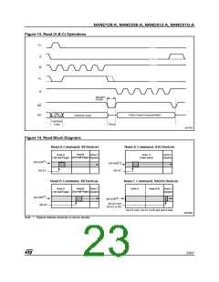
NAND128-A, NAND256-A, NAND512-A, NAND01G-A
Block Erase
are required to input the block address. The
first cycle (A0 to A7) is not required as only
addresses A14 to A26 (highest address
depends on device density) are valid, A9 to
A13 are ignored. In the last address cycle I/O2
to I/O7 must be set to VIL.
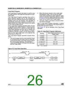
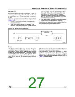
Erase operations are done one block at a time. An
erase operation sets all of the bits in the ad-
dressed block to ‘1’. All previous data in the block
is lost.
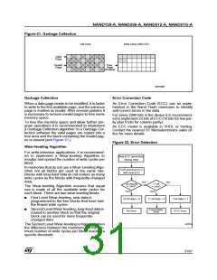
An erase operation consists of three steps (refer to
Figure 19.):
1. One bus cycle is required to setup the Block
Erase command.
2. Only three bus cycles for 512Mb and 1Gb
devices, or two for 128Mb and 256Mb devices
3. One bus cycle is required to issue the confirm
command to start the P/E/R Controller.
Once the erase operation has completed the Sta-
tus Register can be checked for errors.
Figure 19. Block Erase Operation
tBLBH3
(Erase Busy time)
RB
Busy
Block Address
Inputs
I/O
60h
D0h
70h
SR0
Confirm
Code
Read Status Register
Block Erase
Setup Code
ai07593
Reset
The Reset command is used to reset the Com-
mand Interface and Status Register. If the Reset
command is issued during any operation, the op-
eration will be aborted. If it was a program or erase
operation that was aborted, the contents of the
memory locations being modified will no longer be
valid as the data will be partially programmed or
erased.
If the device has already been reset then the new
Reset command will not be accepted.
The Ready/Busy signal goes Low for tBLBH4 after
the Reset command is issued. The value of tBLBH4
depends on the operation that the device was per-
forming when the command was issued, refer to
Table 21. for the values.
27/57

 STMICROELECTRONICS [ ST ]