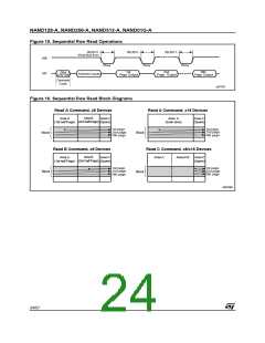
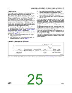
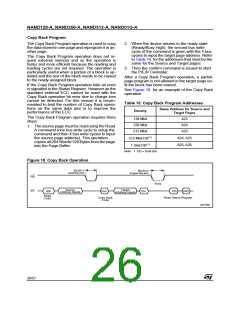
NAND128-A, NAND256-A, NAND512-A, NAND01G-A
Read Status Register
The Status Register bits are summarized in Table
11., Status Register Bits. Refer to Table 11. in
conjunction with the following text descriptions.
The device contains a Status Register which pro-
vides information on the current or previous Pro-
gram or Erase operation. The various bits in the
Status Register convey information and errors on
the operation.
The Status Register is read by issuing the Read
Status Register command. The Status Register in-
formation is present on the output data bus (I/O0-
I/O7) on the falling edge of Chip Enable or Read
Enable, whichever occurs last. When several
memories are connected in a system, the use of
Chip Enable and Read Enable signals allows the
system to poll each device separately, even when
the Ready/Busy pins are common-wired. It is not
necessary to toggle the Chip Enable or Read En-
able signals to update the contents of the Status
Register.
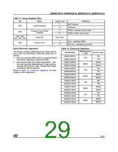
Write Protection Bit (SR7). The Write Protection
bit can be used to identify if the device is protected
or not. If the Write Protection bit is set to ‘1’ the de-
vice is not protected and program or erase opera-
tions are allowed. If the Write Protection bit is set
to ‘0’ the device is protected and program or erase
operations are not allowed.
P/E/R Controller Bit (SR6). The Program/Erase/
Read Controller bit indicates whether the P/E/R
Controller is active or inactive. When the P/E/R
Controller bit is set to ‘0’, the P/E/R Controller is
active (device is busy); when the bit is set to ‘1’, the
P/E/R Controller is inactive (device is ready).
Error Bit (SR0). The Error bit is used to identify if
any errors have been detected by the P/E/R Con-
troller. The Error Bit is set to ’1’ when a program or
erase operation has failed to write the correct data
to the memory. If the Error Bit is set to ‘0’ the oper-
ation has completed successfully.
After the Read Status Register command has
been issued, the device remains in Read Status
Register mode until another command is issued.
Therefore if a Read Status Register command is
issued during a Random Read cycle a new read
command must be issued to continue with a Page
Read or Sequential Row Read operation.
SR5, SR4, SR3, SR2 and SR1 are Reserved.
28/57

 STMICROELECTRONICS [ ST ]