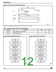
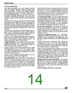
M59PW1282
After the Chip Erase operation has completed the
memory will return to the Read Mode, unless an
error has occurred. When an error occurs the
memory will continue to output the Status Regis-
ter. A Read/Reset command must be issued to re-
set the error condition and return to Read Mode.
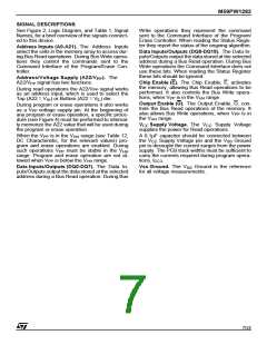
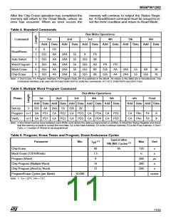
Table 4. Standard Commands
Bus Write Operations
Command
1st
2nd
Data
3rd
4th
5th
6th
Add
X
Data
F0
Add
Add
Data
Add
Data
Add
Data
Add
Data
1
3
3
4
6
6
Read/Reset
555
555
555
555
555
AA
AA
AA
AA
AA
2AA
2AA
2AA
2AA
2AA
55
55
55
55
55
X
F0
90
A0
80
80
Auto Select
Word Program
Block Erase
Chip Erase
555
555
555
555
PA
555
555
PD
AA
AA
2AA
2AA
55
55
BA
30
10
555
Note: X Don’t Care, PA Program Address, PD Program Data, BA Any address in the Block. All values in the table are in hexadecimal. The
Command Interface only uses A0-A10 and DQ0-DQ7 to verify the commands; A11-A21, DQ8-DQ15 are Don’t Care.
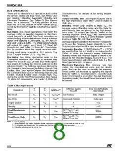
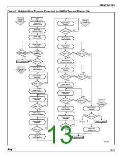
Table 5. Multiple Word Program Command
Bus Write Operations
Phase
1st
Add Data Add Data Add Data Add Data Add Data
555 AA 2AA 55 555 20
2nd
3rd
4th
5th
nth
Final
Add Data Add Data
Set-Up
3
Program n+1 SA PD1 CA PD2 CA PD3 CA PD4 CA PD5
Verify n+1 SA PD1 CA PD2 CA PD3 CA PD4 CA PD5
CA PAn
CA PAn
FA
FA
X
X
Note: A Bus Read must be done between each Write cycle where the data is programmed or verified, to Read the Status Register and check
that the memory is ready to accept the next data. SA is the Start Address. CA is the Continue Address. FA is the Final Address. X Don’t
Care, n = number of Words to be programmed.
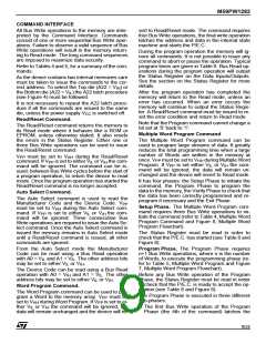
Table 6. Program, Erase Times and Program, Erase Endurance Cycles
Typical after
(1)
Parameter
Min
Max
Unit
Typ
80
(1)
10k W/E Cycles
Chip Erase
85
120
6
s
Block Erase (128 KWords)
Program (Word)
1.5
9
s
200
280
280
µs
Chip Program (Multiple Word)
Chip Program (Word by Word)
Program/Erase Cycles (per Block)
16
72
s
s
10,000
cycles
Note: 1. T = 25°C, V = 12V.
A
PP
11/24

 STMICROELECTRONICS [ ST ]