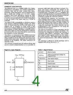
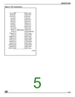
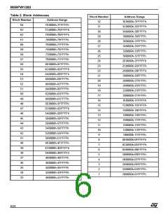
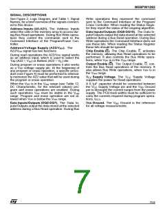
M59PW1282
BUS OPERATIONS
There are six standard bus operations that control
the device. These are Bus Read, Bus Write, Out-
put Disable, Standby, Automatic Standby and
Electronic Signature. See Tables 3, Bus Opera-
tions, for a summary. Typically glitches of less
than 5ns on Chip Enable or Write Enable are ig-
nored by the memory and do not affect bus opera-
tions.
Bus Read. Bus Read operations read from the
memory cells, or specific registers in the Com-
mand Interface. A valid Bus Read operation in-
volves setting the desired address on the Address
Characteristics, for details of the timing require-
ments.
Output Disable. The Data Inputs/Outputs are in
the high impedance state when Output Enable is
High, V .
IH
Standby. When Chip Enable is High, V , the
IH
memory enters Standby mode and the Data In-
puts/Outputs pins are placed in the high-imped-
ance state. To reduce the Supply Current to the
Standby Supply Current, I
, Chip Enable should
CC2
be held within V ± 0.2V. For the Standby current
CC
level see Table 12, DC Characteristics.
During program operation the memory will contin-
Inputs and applying a Low signal, V , to Chip En-
IL
able and Output Enable. The Data Inputs/Outputs
will output the value, see Figure 12, Read AC
Waveforms, and Table 12, Read AC Characteris-
tics, for details of when the output becomes valid.
ue to use the Program Supply Current, I
, for
CC3
Program operation until the operation completes.
Automatic Standby. If CMOS levels (V ± 0.2V)
CC
are used to drive the bus and the bus is inactive for
150ns or more the memory enters Automatic
Standby where the internal Supply Current is re-
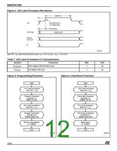
During read array operations A22 selects Top
(A22 = V ) or Bottom (A22 = V ) die.
IH
IL
Bus Write. Bus Write operations write to the
Command Interface. Bus Write is enabled only
duced to the Standby Supply Current, I
. The
CC2
Data Inputs/Outputs will still output data if a Bus
Read operation is in progress.
when V is set to V . A valid Bus Write opera-
PP
HH
tion begins by setting the desired address on the
Address Inputs. The Address Inputs are latched by
the Command Interface on the falling edge of Chip
Enable. The Data Inputs/Outputs are latched by
the Command Interface on the rising edge of Chip
Electronic Signature. The memory has two
codes, the manufacturer code and the device
code, that can be read to identify the memory.
These codes can be read by applying the signals
listed in Tables 3, Bus Operations, once the Auto
Select Command is executed. To exit Electronic
Signature mode, the Read/Reset command must
be issued.
Enable. Output Enable must remain High, V ,
IH
during the whole Bus Write operation. See Figure
12, Write AC Waveforms, and Table 14, Write AC
Table 3. Bus Operations
Address Inputs
A0-A21
Data Inputs/Outputs
DQ15-DQ0
(2)
PP
Operation
Bus Read
E
G
A22/V
(3)
V
V
IL
Cell Address
Data Output
V /V
IL
IL
IL IH
(4)
V
V
IH
V
IH
Bus Write
Command Address
Data Input
Hi-Z
V
HH
Output Disable
Standby
X
X
X
X
X
V
IH
X
Hi-Z
A0 = V , A1 = V ,
Read Manufacturer
Code
IL
IL
V
V
V
V
0020h
88AAh
IL
IL
IL
IL
HH
Others V or V
IL
IH
A0 = V , A1 = V ,
IH
IL
V
V
HH
Read Device Code
Others V or V
IL
IH
Note: 1. X = V or V
.
IH
IL
2. When reading the Status Register during a program operation A22/V must be kept at V
.
HH
PP
3. V enables the Bottom die, V enables the Top die during read array operation.
IL
IH
4. V after latching A22 at V or V .
IH
HH
IL
8/24

 STMICROELECTRONICS [ ST ]