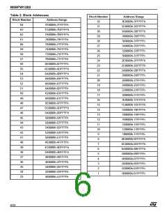
M59PW1282
SIGNAL DESCRIPTIONS
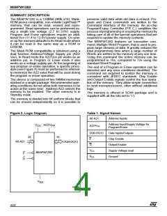
See Figure 2, Logic Diagram, and Table 1, Signal
Names, for a brief overview of the signals connect-
ed to this device.
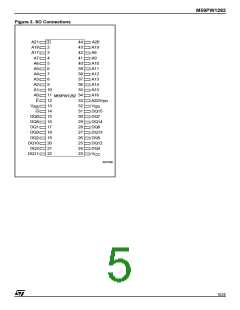
Address Inputs (A0-A21). The Address Inputs
select the cells in the memory array to access dur-
ing Bus Read operations. During Bus Write opera-
tions they control the commands sent to the
Command Interface of the Program/Erase Con-
troller.
Write operations they represent the command
sent to the Command Interface of the Program/
Erase Controller. When reading the Status Regis-
ter they report the status of the ongoing algorithm.
Data Inputs/Outputs (DQ8-DQ15). The Data In-
puts/Outputs output the data stored at the selected
address during a Bus Read operation. During Bus
Write operations the Command Interface does not
use these bits. When reading the Status Register
these bits should be ignored.
Address/Voltage Supply (A22/V ). The
PP
A22/V signal has two functions.
During read operations the A22/V signal works
as an address input, which is used to select the
Chip Enable (E). The Chip Enable, E, activates
the memory, allowing Bus Read operations to be
performed. It also controls the Bus Write opera-
PP
PP
tions, when V is in the V range.
PP
HH
Top (A22 = V ) or Bottom (A22 = V ) die.
IH
IL
Output Enable (G). The Output Enable, G, con-
trols the Bus Read operations of the memory. It
During program or erase operations it also works
as a V voltage supply pin. At the beginning of
PP
also allows Bus Write operations, when V is in
PP
any program or erase operation, a specific proce-
dure (see Figure 4) must be performed to internal-
ly memorize the A22 value that will be used during
the program or erase operation.
the V range.
HH
V
Supply Voltage. The V
Supply Voltage
CC
CC
supplies the power for Read operations.
When the V is in the V
DC Characteristic, for the relevant values) pro-
range (see Table 12,
HH
A 0.1µF capacitor should be connected between
PP
the V
Supply Voltage pin and the V Ground
CC SS
gram and erase operations are enabled. During
pin to decouple the current surges from the power
supply. The PCB track widths must be sufficient to
carry the currents required during program opera-
such operations V
must be stable in the V
HH
PP
range. Program and erase operation are not al-
lowed when V is below the V range.
tions, I .
PP
HH
CC3
Data Inputs/Outputs (DQ0-DQ7). The Data In-
puts/Outputs output the data stored at the selected
address during a Bus Read operation. During Bus
Vss Ground. The V
for all voltage measurements.
Ground is the reference
SS
7/24

 STMICROELECTRONICS [ ST ]