M59PW1282
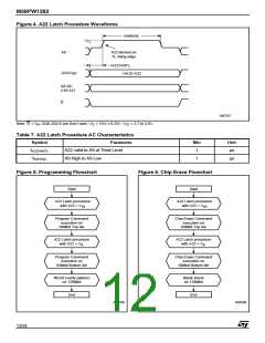
Figure 4. A22 Latch Procedure Waveforms
tA9HA9L
V
TL
A9
A22 latched on
TL rising edge
tA22VA9TL
A22/V
VALID A22
PP
A0-A8;
A10-A21
E
AI07257
Note: G = V ; DQ0–DQ15 are Don’t care; V = 10.5 ± 0.25V; V = 2.7 to 3.6V.
IH
TL
CC
Table 7. A22 Latch Procedure AC Characteristics
Symbol
Parameter
A22 valid to A9 at Third Level
A9 High to A9 Low
Min
1
Unit
t
µs
µs
A22VA9TL
t
1
A9HA9L
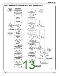
Figure 5. Programming Flowchart
Figure 6. Chip Erase Flowchart
Start
Start
A22 Latch procedure
A22 Latch procedure
with A22 = V
with A22 = V
IH
IH
Program Command
execution on
Chip Erase Command
execution on
64Mbit Top die
64Mbit Top die
A22 Latch procedure
A22 Latch procedure
with A22 = V
with A22 = V
IL
IL
Program Command
execution on
Chip Erase Command
execution on
64Mbit Bottom die
64Mbit Bottom die
READ (verify pattern)
on 128Mbit
Blank check
on 128Mbit
End
End
AI08208
AI08209
12/24

 STMICROELECTRONICS [ ST ]