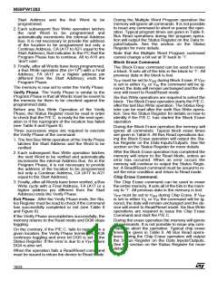
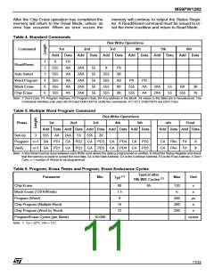
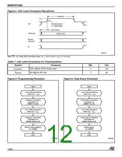
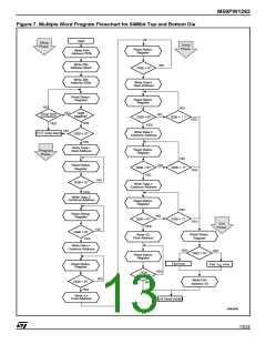
M59PW1282
STATUS REGISTER
Bus Read operations from any address always
read the Status Register during Program and
Erase operations. The bits in the Status Register
are summarized in Table 8, Status Register Bits.
Data Polling Bit (DQ7). The Data Polling Bit can
be used to identify whether the P/E.C. has suc-
cessfully completed its operation. The Data Poll-
ing Bit is output on DQ7 when the Status Register
is read.
Note that the Program command cannot change a
bit set to ’0’ back to ’1’ and attempting to do so will
set DQ5 to ‘1’. A Bus Read operation to that ad-
dress will show the bit is still ‘0’. One of the Erase
commands must be used to set all the bits in a
block or in the whole memory from ’0’ to ’1’.
V
Status Bit (DQ4). The V Status Bit can be
PP
PP
used to identify if any Program or Erase operation
has failed due to a V error. If V falls below V
PP
PP
HH
during any Program or Erase operation, the oper-
ation aborts and DQ4 is set to ‘1’. If V remains at
During a Word Program operation the Data Polling
Bit outputs the complement of the bit being pro-
grammed to DQ7. After successful completion of
the Word Program operation the memory returns
to Read mode and Bus Read operations from the
address just programmed output DQ7, not its com-
plement.
During Erase operations the Data Polling Bit out-
puts ’0’, the complement of the erased state of
DQ7. After successful completion of the Erase op-
eration the memory returns to Read Mode.
PP
V
throughout the Program or Erase operation,
HH
the operation completes and DQ4 is set to ‘0’.
Erase Timer Bit (DQ3). The Erase Timer Bit can
be used to identify the start of P/E.C. operation
during a Block Erase command. Once the P/E.C.
starts erasing the Erase Timer Bit is set to ’1’. The
Erase Timer Bit is output on DQ3 when the Status
Register is read.
Alternative Toggle Bit (DQ2). The Alternative
Toggle Bit can be used to monitor the P/E.C. dur-
ing Block Erase operations. The Alternative Tog-
gle Bit is output on DQ2 when the Status Register
is read.
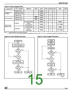
Figure 8, Data Polling Flowchart, gives an exam-
ple of how to use the Data Polling Bit. A Valid Ad-
dress is the address being programmed or an
address within the block being erased.
During Block Erase operations the Toggle Bit
changes from ’0’ to ’1’ to ’0’, etc., with successive
Bus Read operations from addresses within the
block being erased. Once the operation completes
the memory returns to Read mode.
After an Erase operation that causes the Error Bit
to be set, the Alternative Toggle Bit can be used to
identify where the error occurred. The Alternative
Toggle Bit changes from ’0’ to ’1’ to ’0’, etc. with
successive Bus Read Operations from addresses
within a block that has not erased correctly. The
Alternative Toggle Bit does not change if the ad-
dressed block has erased correctly.
Multiple Word Program Bit (DQ0). The Multiple
Word Program Bit can be used to indicate whether
the P/E.C. is active or inactive during Multiple
Word Program. When the P/E.C. has written one
Word and is ready to accept the next Word, the bit
is set to ‘0’.
Toggle Bit (DQ6). The Toggle Bit can be used to
identify whether the P/E.C. has successfully com-
pleted its operation. The Toggle Bit is output on
DQ6 when the Status Register is read.
During Program and Erase operations the Toggle
Bit changes from ’0’ to ’1’ to ’0’, etc., with succes-
sive Bus Read operations at any address. After
successful completion of the operation the memo-
ry returns to Read mode.
Figure 9, Data Toggle Flowchart, gives an exam-
ple of how to use the Data Toggle Bit.
Error Bit (DQ5). The Error Bit can be used to
identify errors detected by the P/E.C. The Error Bit
is set to ’1’ when a Program, Block Erase or Chip
Erase operation fails to write the correct data to
the memory. If the Error Bit is set a Read/Reset
command must be issued before other commands
are issued. The Error bit is output on DQ5 when
the Status Register is read.
Status Register Bit DQ1 is reserved.
14/24

 STMICROELECTRONICS [ ST ]