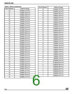
M59PW1282
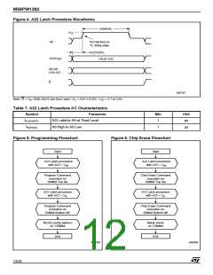
Start Address and the first Word to be
programmed.
During the Multiple Word Program operation the
memory will ignore all commands. It is not possible
to issue any command to abort or pause the oper-
ation. Typical program times are given in Table 6.
Bus Read operations during the program opera-
tion will output the Status Register on the Data In-
puts/Outputs. See the section on the Status
Register for more details.
2. Each subsequent Bus Write operation latches
the next Word to be programmed and
automatically increments the internal Address
Bus. It is not necessary to provide the address
of the location to be programmed but only a
Continue Address, CA (A17 to A21 equal to the
Start Address), that indicates to the PC that the
Program Phase has to continue. A0 to A16 are
‘don’t care’.
Note that the Multiple Word Program command
cannot change a bit set at ’0’ back to ’1’.
Block Erase Command.
3. Finally, after all Words have been programmed,
The Block Erase command can be used to erase
a block. It sets all of the bits in the block to ’1’. All
previous data in the block is lost.
th
a Bus Write operation (the (n+1) ) with a Final
Address, FA (A17 or a higher address pin
different from the Start Address), ends the
Program Phase.
V
must be set to V during Block Erase. If V
HH PP
PP
is set to either V or V the command will be ig-
IL
IH
The memory is now set to enter the Verify Phase.
nored, the data will remain unchanged and the de-
vice will revert to Read/Reset mode.
Verify Phase. The Verify Phase is similar to the
Program Phase in that all Words must be resent to
the memory for them to be checked against the
programmed data.
Before any Bus Write Operation of the Verify
Phase, the Status Register must be read in order
to check that the P/E.C. is ready for the next oper-
ation or if the reprogram of the location has failed
(see Table 8 and Figure 8).
Six Bus Write operations are required to select the
block . The Block Erase operation starts the P/E.C.
after the last Bus Write operation. The Status Reg-
ister can be read after the sixth Bus Write opera-
tion. See the Status Register for details on how to
identify if the P/E.C. has started the Block Erase
operation.
During the Block Erase operation the memory will
ignore all commands. Typical block erase times
are given in Table 6. All Bus Read operations dur-
ing the Block Erase operation will output the Sta-
tus Register on the Data Inputs/Outputs. See the
section on the Status Register for more details.
Three successive steps are required to execute
the Verify Phase of the command:
1. The first Bus Write operation of the Verify Phase
latches the Start Address and the Word to be
verified.
After the Block Erase operation has completed the
memory will return to the Read Mode, unless an
error has occurred. When an error occurs the
memory will continue to output the Status Regis-
ter. A Read/Reset command must be issued to re-
set the error condition and return to Read mode.
2. Each subsequent Bus Write operation latches
the next Word to be verified and automatically
increments the internal Address Bus. As in the
Program Phase, it is not necessary to provide
the address of the location to be programmed
but only a Continue Address, CA (A17 to A21
equal to the Start Address).
Chip Erase Command.
3. Finally, after all Words have been verified, a Bus
Write cycle with a Final Address, FA (A17 or a
higher address pin different from the Start
Address) ends the Verify Phase.
The Chip Erase command can be used to erase
the entire memory. It sets all of the bits in the mem-
ory to ’1’. All previous data in the memory is lost.
V
must be set to V during Chip Erase. If V
HH PP
PP
Exit Phase. After the Verify Phase ends, the Sta-
tus Register must be read to check if the command
has successfully completed or not (see Table 8
and Figure 8).
If the Verify Phase accomplishes successfully, the
memory returns to the Read mode and DQ6 stops
toggling.
On the contrary, if the P/E.C. fails to reprogram a
given location, the Verify Phase terminates, DQ6
continues toggling and error bit DQ5 is set in the
is set to either V or V the command will be ig-
IL IH
nored, the data will remain unchanged and the de-
vice will revert to Read/Reset mode. Six Bus Write
operations are required to issue the Chip Erase
Command and start the P/E.C.
During the erase operation the memory will ignore
all commands. It is not possible to issue any com-
mand to abort the operation. Typical chip erase
times are given in Table 6. All Bus Read opera-
tions during the Chip Erase operation will output
the Status Register on the Data Inputs/Outputs.
See the section on the Status Register for more
details.
Status Register. If the error is due to a V failure
PP
DQ4 is also set.
When the operation fails a Read/Reset command
must be issued to return the device to Read mode.
10/24

 STMICROELECTRONICS [ ST ]