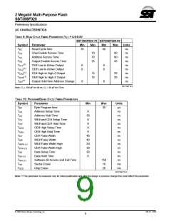
2 Megabit Multi-Purpose Flash
SST39SF020
Preliminary Specifications
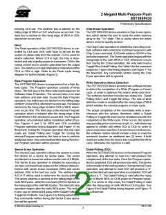
Toggle Bit (DQ6)
orpower-down.AnyEraseoperationrequirestheinclusion
of six byte load sequence. The SST39SF020 device is
shipped with the software data protection permanently
enabled. See Table 4 for the specific software command
codes. During SDP command sequence, invalid com-
mands will abort the device to read mode, within TRC.
During the internal Program or Erase operation, any con-
secutive attempts to read DQ6 will produce alternating 0’s
and 1’s, i.e., toggling between 0 and 1. The Toggle Bit will
beginwith“1”. WhentheinternalProgramorEraseopera-
tion is completed, the toggling will stop. The device is then
readyforthenextoperation.TheToggleBitisvalidafterthe
rising edge of fourth WE# (or CE#) pulse for Program
operation. For Sector or Chip Erase, the Toggle Bit is valid
after the rising edge of sixth WE# (or CE#) pulse. See
Figure 7 for Toggle Bit timing diagram and Figure 15 for a
flowchart.
1
2
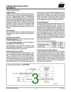
Product Identification
Theproductidentificationmodeidentifiesthedeviceasthe
SST39SF020 and manufacturer as SST. This mode may
be accessed by hardware or software operations. The
hardware operation is typically used by a programmer to
identify the correct algorithm for the SST39SF020 device.
Users may wish to use the software product identification
operation to identify the part (i.e., using the device code)
whenusingmultiplemanufacturersinthesamesocket.For
details, see Table 3 for hardware operation or Table 4 for
softwareoperation,Figure10forthesoftwareIDentryand
read timing diagram and Figure 16 for the ID entry com-
mand sequence flowchart.
3
4
Data Protection
The SST39SF020 device provides both hardware and
softwarefeaturestoprotectnonvolatiledatafrominadvert-
ent writes.
5
Hardware Data Protection
Noise/Glitch Protection: A WE# or CE# pulse of less than
5 ns will not initiate a write cycle.
6
TABLE 1: PRODUCT IDENTIFICATION TABLE
7
VCC Power Up/Down Detection: The write operation is
inhibited when VCC is less than 2.5V.
Address
0000H
Data
Manufacturer’s Code
Device Code
BF H
Write Inhibit Mode: Forcing OE# low, CE# high, or WE#
highwillinhibittheWriteoperation.Thispreventsinadvert-
ent writes during power-up or power-down.
8
0001H
B6 H
326 PGM T1.2
Product Identification Mode Exit/Reset
9
Software Data Protection (SDP)
In order to return to the standard read mode, the Software
Product Identification mode must be exited. Exiting is
accomplished by issuing the Exit ID command sequence,
which returns the device to the Read operation. Please
notethatthesoftwareresetcommandisignoredduringan
internal Program or Erase operation. See Table 4 for
software command codes, Figure 11 for timing waveform
and Figure 16 for a flowchart.
The SST39SF020 provides the JEDEC approved soft-
ware data protection scheme for all data alteration opera-
tions, i.e., Program and Erase. Any Program operation
requires the inclusion of a series of three byte sequence.
The three byte-load sequence is used to initiate the Pro-
gram operation, providing optimal protection from inad-
vertent write operations, e.g., during the system power-up
10
11
12
13
14
15
16
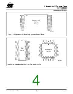
FUNCTIONAL BLOCK DIAGRAM OF SST39SF020
2,097,152 bit
EEPROM
Cell Array
X-Decoder
A
- A
0
17
Address Buffers & Latches
Control Logic
Y-Decoder
CE#
OE#
WE#
I/O Buffers and Data Latches
DQ - DQ
7
0
326 ILL B1.3
© 1998 Silicon Storage Technology, Inc.
326-10 12/98
3

 SST [ SILICON STORAGE TECHNOLOGY, INC ]