2 Megabit Multi-Purpose Flash
SST39SF020
Preliminary Specifications
keeping CE# low. The address bus is latched on the
falling edge of WE# or CE#, whichever occurs last. The
data bus is latched on the rising edge of WE# or CE#,
whichever occurs first.
Chip-Erase Operation
The SST39SF020 device provides a Chip-Erase opera-
tion, which allows the user to erase the entire memory
array to the “1’s” state. This is useful when the entire
device must be quickly erased.
Read
The Chip Erase operation is initiated by executing a six-
byte software data protection command sequence with
Chip Erase command (10H) with address 5555H in the
lastbytesequence. TheEraseoperationbeginswiththe
rising edge of the sixth WE# or CE#, whichever occurs
first. During the Erase operation, the only valid read is
ToggleBitorData#Polling.SeeTable4forthecommand
sequence, Figure9fortimingdiagram, andFigure17for
the flowchart. Any commands written during the Chip
Erase operation will be ignored.
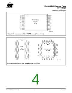
The Read operation of the SST39SF020 device is con-
trolled by CE# and OE#, both have to be low for the
system to obtain data from the outputs. CE# is used for
device selection. When CE# is high, the chip is dese-
lected and only standby power is consumed. OE# is the
output control and is used to gate data from the output
pins.Thedatabusisinhighimpedancestatewheneither
CE# or OE# is high. Refer to the Read cycle timing
diagram for further details (Figure 3).
Byte Program Operation
Write Operation Status Detection
The SST39SF020 device is programmed on a byte-by-
byte basis. The Program operation consists of three
steps. The first step is the three-byte-load sequence for
Software Data Protection. The second step is to load
byte address and byte data. During the Byte Program
operation, the addresses are latched on the falling edge
of either CE# or WE#, whichever occurs last. The data is
latched on the rising edge of either CE# or WE#, which-
ever occurs first. The third step is the internal Program
operation which is initiated after the rising edge of the
fourthWE#orCE#, whicheveroccursfirst. TheProgram
operation, onceinitiated, willbecompleted, within30µs.
See Figures 4 and 5 for WE# and CE# controlled
Program operation timing diagrams and Figure 14 for
flowcharts. During the Program operation, the only valid
reads are Data# Polling and Toggle Bit. During the
internal Program operation, the host is free to perform
additionaltasks. Anycommandswrittenduringtheinter-
nal Program operation will be ignored.
The SST39SF020 device provides two software means
to detect the completion of a Write (Program or Erase)
cycle, in order to optimize the system write cycle time.
The software detection includes two status bits : Data#
Polling (DQ7) and Toggle Bit (DQ6). The end of write
detection mode is enabled after the rising edge of WE#
which initiates the internal program or erase cycle.
The actual completion of the nonvolatile write is asyn-
chronous with the system; therefore, either a Data#
Polling or Toggle Bit read may be simultaneous with the
completion of the Write cycle. If this occurs, the system
maypossiblygetanerroneousresult,i.e.,validdatamay
appear to conflict with either DQ7 or DQ6. In order to
preventspuriousrejection,ifanerroneousresultoccurs,
the software routine should include a loop to read the
accessed location an additional two (2) times. If both
reads are valid, then the device has completed the Write
cycle, otherwise the rejection is valid.
Sector Erase Operation
Data# Polling (DQ7)
The Sector Erase operation allows the system to erase
the device on a sector by sector basis. The sector
architecture is based on uniform sector size of 4 KByte.
The Sector Erase operation is initiated by executing a
six-byte-commandloadsequenceforsoftwaredatapro-
tection with sector erase command (30H) and sector
address (SA) in the last bus cycle. The address lines
A12-A17 will be used to determine the sector address.
The sector address is latched on the falling edge of the
sixthWE#pulse,whilethecommand(30H)islatchedon
therisingedgeofthesixthWE#pulse.TheinternalErase
operation begins after the sixth WE# pulse. The end of
Erase can be determined using either Data# Polling or
Toggle Bit methods. See Figure 8 for timing waveforms.
Any commands written during the Sector Erase opera-
tion will be ignored.
WhentheSST39SF020deviceisintheinternalProgram
operation, any attempt to read DQ7 will produce the
complement of the true data. Once the Program opera-
tioniscompleted,DQ7 willproducetruedata.Thedevice
isthenreadyforthenextoperation.DuringinternalErase
operation, any attempt to read DQ7 will produce a ‘0’.
OncetheinternalEraseoperationiscompleted,DQ7will
produce a ‘1’. The Data# Polling is valid after the rising
edge of fourth WE# (or CE#) pulse for Program opera-
tion. For sector or chip erase, the Data# Polling is valid
after the rising edge of sixth WE# (or CE#) pulse. See
Figure 6 for Data# Polling timing diagram and Figure 15
for a flowchart.
© 1998 Silicon Storage Technology, Inc.
326-10 12/98
2

 SST [ SILICON STORAGE TECHNOLOGY, INC ]