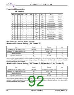
A d v a n c e I n f o r m a t i o n
AC Operating Conditions
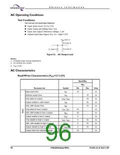
Test Conditions
Test Load and Test Input/Output Reference
Input pulse level: 0.4 to 2.2V
Input rising and falling time: 5ns
Input and output reference voltage: 1.5V
Output load (See Figure 32): CL= 30pF+1TTL
V
(note 3)
TM
R2 (note 2)
R1 (note 2)
CL (note 1)
Figure 32. AC Output Load
Notes:
1. Including scope and jig capacitance.
2. R1=3070Ω, R2=3150Ω.
3. VTM =2.8V.
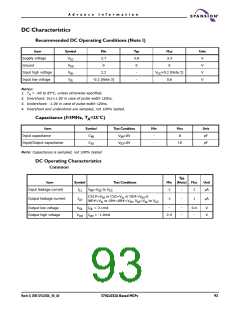
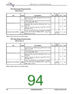
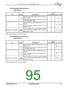
AC Characteristics
Read/Write Characteristics (VCC=2.7-3.3V)
Speed Bins
70ns
Parameter List
Read cycle time
Symbol
tRC
tAA
tCO1, tCO2
tOE
Min
Max
-
Units
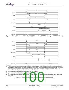
ns
ns
ns
ns
ns
ns
ns
ns
ns
ns
ns
ns
70
-
Address access time
70
70
35
70
-
Chip select to output
-
Output enable to valid output
LB#, UB# Access Time
-
tBA
-
Chip select to low-Z output
LB#, UB# enable to low-Z output
Output enable to low-Z output
Chip disable to high-Z output
UB#, LB# disable to high-Z output
Output disable to high-Z output
Output hold from address change
tLZ1, tLZ2
tBLZ
10
10
5
-
tOLZ
-
tHZ1, tHZ2
tBHZ
0
25
25
25
-
0
tOHZ
0
tOH
10
96
S71GL032A Based MCPs
S71GL032A_00_A0 March 31, 2005

 SPANSION [ SPANSION ]