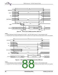
A d v a n c e I n f o r m a t i o n
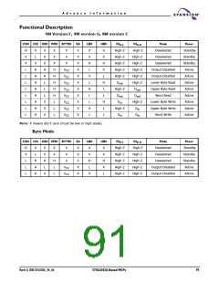
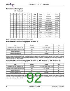
Functional Description
8M Version D
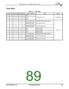
CS1# CS2 OE# WE#
LB#
X
X
H
L
UB#
X
IO0~8
High-Z
High-Z
High-Z
High-Z
High-Z
Dout
IO9~16
High-Z
High-Z
High-Z
High-Z
High-Z
High-Z
Dout
Mode
Power
Standby
Standby
Standby
Active
H
X
X
L
L
L
L
L
L
L
L
X
L
X
X
X
H
H
L
X
X
X
H
H
H
H
H
L
Deselected
X
Deselected
X
H
H
H
H
H
H
H
H
H
X
Deselected
Output Disabled
Output Disabled
Lower Byte Read
Upper Byte Read
Word Read
X
L
L
Active
H
L
Active
L
H
L
High-Z
Dout
Active
L
L
Dout
Active
X
X
X
L
H
L
Din
High-Z
Din
Lower Byte Write
Upper Byte Write
Word Write
Active
L
H
L
High-Z
Din
Active
L
L
Din
Active
Note: X means don’t care (must be low or high state).
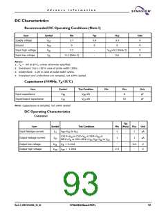
Absolute Maximum Ratings (4M Version F)
Item
Symbol
VIN,VOUT
VCC
Ratings
Unit
Voltage on any pin relative to VSS
Voltage on VCC supply relative to VSS
Power Dissipation
-0.2 to VCC+0.3V
V
V
-0.2 to 4.0V
1.0
PD
W
Operating Temperature
TA
-40 to 85
°C
Stresses greater than those listed under “Absolute Maximum Ratings” may cause permanent damage to the device. Functional
operation should be restricted to recommended operating condition. Exposure to absolute maximum rating conditions for
extended periods may affect reliability.
Absolute Maximum Ratings (4M Version G, 8M Version C, 8M Version D)
Item
Symbol
VIN,VOUT
VCC
Ratings
-0.2 to VCC+0.3V (Max. 3.6V)
-0.2 to 3.6V
Unit
V
Voltage on any pin relative to VSS
Voltage on VCC supply relative to VSS
Power Dissipation
V
PD
1.0
W
Operating Temperature
TA
-40 to 85
°C
Stresses greater than those listed under “Absolute Maximum Ratings” may cause permanent damage to the device. Functional
operation should be restricted to recommended operating condition. Exposure to absolute maximum rating conditions for
extended periods may affect reliability.
92
S71GL032A Based MCPs
S71GL032A_00_A0 March 31, 2005

 SPANSION [ SPANSION ]