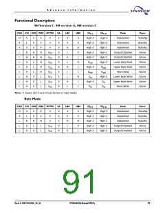
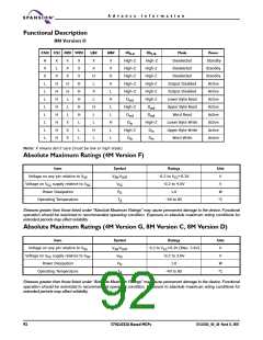
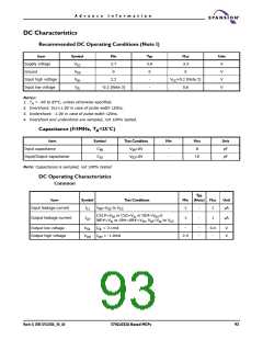
A d v a n c e I n f o r m a t i o n
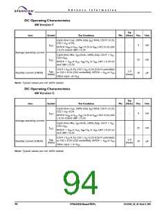
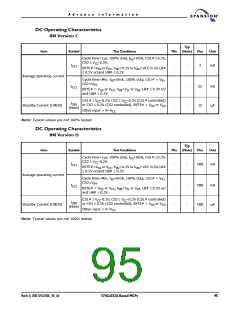
DC Operating Characteristics
8M Version C
Typ
Item
Symbol
Test Conditions
Min
(Note)
Max
Unit
Cycle time=1µs, 100% duty, IIO=0mA, CS1# ≤ 0.2V,
CS2
BYTE#=VSS or VCC, VIN
0.2V or/and UB# 0.2V
≥ VCC-0.2V,
ICC1
-
-
3
mA
≤
0.2V or VIN ≥ VCC-0.2V, LB#
≤
≤
Average operating current
Standby Current (CMOS)
Cycle time=Min, IIO=0mA, 100% duty, CS1# = VIL,
CS2=VIH,
ICC2
-
-
-
-
22
15
mA
µA
BYTE# = VSS or VCC, VIN=VIL or VIH, LB#
and UB# 0.2V
≤ 0.2V or/
≤
CS1#
≥ VCC-0.2V, CS2 ≥ VCC-0.2V (CS1# controlled)
ISB1
(Note)
or CS2 0.2V (CS2 controlled), BYTE# = VSS or VCC
≤
,
Other input = 0~VCC
Note: Typical values are not 100% tested.
DC Operating Characteristics
8M Version D
Typ
Item
Symbol
Test Conditions
Min
(Note)
Max
Unit
Cycle time=1µs, 100% duty, IIO=0mA, CS1# ≤ 0.2V,
CS2
BYTE#=VSS or VCC, VIN
0.2V or/and UB# 0.2V
≥ VCC-0.2V,
ICC1
-
-
TBD
mA
≤
0.2V or VIN ≥ VCC-0.2V, LB#
≤
≤
Average operating current
Cycle time=Min, IIO=0mA, 100% duty, CS1# = VIL,
CS2=VIH,
ICC2
-
-
-
-
TBD
TBD
mA
µA
BYTE# = VSS or VCC, VIN=VIL or VIH, LB#
and UB# 0.2V
≤ 0.2V or/
≤
CS1#
≥ VCC-0.2V, CS2 ≥ VCC-0.2V (CS1# controlled)
ISB1
(Note)
or CS2 0.2V (CS2 controlled), BYTE# = VSS or VCC
≤
,
Standby Current (CMOS)
Other input = 0~VCC
Note: Typical values are not 100% tested.
March 31, 2005 S71GL032A_00_A0
S71GL032A Based MCPs
95

 SPANSION [ SPANSION ]