A d v a n c e I n f o r m a t i o n
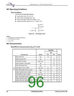
Speed Bins
70ns
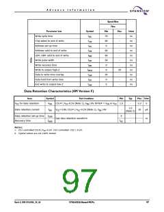
Parameter List
Write cycle time
Symbol
tWC
tCW
tAS
Min
Max
Units
ns
ns
ns
ns
ns
ns
ns
ns
ns
ns
ns
70
60
0
-
-
Chip select to end of write
Address set-up time
-
Address valid to end of write
LB#, UB# valid to end of write
Write pulse width
tAW
60
60
50
0
-
tBW
-
tWP
-
Write recovery time
tWR
tWHZ
tDW
tDH
-
Write to output high-Z
Data to write time overlap
Data hold from write time
End write to output low-Z
0
20
-
30
0
-
tOW
5
-
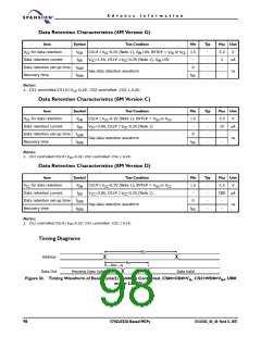
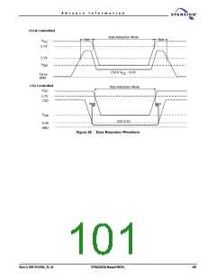
Data Retention Characteristics (4M Version F)
Item
Symbol
Test Condition
Min
Typ
Max Unit
VCC for data retention
VDR
CS1#
≥
VCC-0.2V (Note 1), VIN 0V. BYTE# = VSS or VCC 1.5
≥
-
3.3
10
V
1.0
(Note 2)
Data retention current
IDR
VCC=3.0V, CS1#
≥
VCC-0.2V (Note 1), VIN
≥
0V
-
µA
Data retention set-up time
Recovery time
tSDR
tRDR
0
-
-
-
-
See data retention waveform
ns
tRC
Notes:
1. CS1 controlled:CS1#≥ VCC-0.2V. CS2 controlled: CS2 ≤ 0.2V.
2. Typical values are not 100% tested.
March 31, 2005 S71GL032A_00_A0
S71GL032A Based MCPs
97

 SPANSION [ SPANSION ]