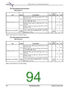
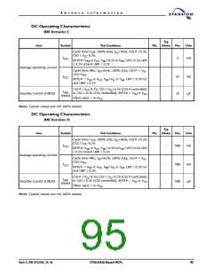
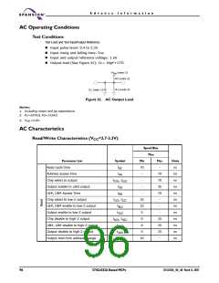
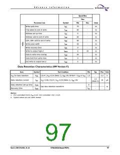
A d v a n c e I n f o r m a t i o n
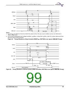
tWC
Address
CS1#
tAS(3)
tCW(2)
tAW
tWR(4)
CS2
UB#, LB#
WE#
tBW
tWP(1)
tDW
Data Valid
tDH
Data in
Data out
High-Z
High-Z
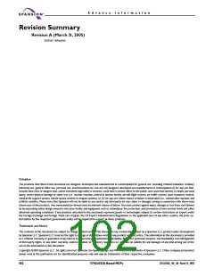
Figure 36. Timing Waveform of Write Cycle(2) (CS# controlled, if BYTE# is Low, Ignore UB#/LB# Timing)
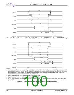
tWC
Address
tCW(2)
tWR(4)
CS1#
tAW
CS2
tCW(2)
tBW
UB#, LB#
tAS(3)
tWP(1)
WE#
tDH
tDW
Data Valid
Data in
Data out
High-Z
High-Z
Notes:
1. A write occurs during the overlap (t ) of low CS1# and low WE#. A write begins when CS1# goes low and WE#
WP
goes low with asserting UB# or LB# for single byte operation or simultaneously asserting UB# and LB# for double
byte operation. A write ends at the earliest transition when CS1# goes high and WE# goes high. The t
measured from the beginning of write to the end of write.
is
WP
2. t
is measured from the CS1# going low to the end of write.
CW
3. t is measured from the address valid to the beginning of write.
AS
4. t
is measured from the end of write to the address change. t
applied in case a write ends as CS1# or WE#
WR
WR
going high.
Figure 37. Timing Waveform of Write Cycle(3) (UB#, LB# controlled)
100
S71GL032A Based MCPs
S71GL032A_00_A0 March 31, 2005

 SPANSION [ SPANSION ]