A d v a n c e I n f o r m a t i o n
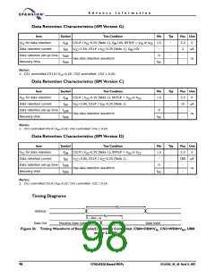
tRC
Address
tOH
tAA
tCO1
CS1#
CS2
tCO2
tBA
tHZ
UB#, LB#
tBHZ
tOHZ
tOE
OE#
tOLZ
tBLZ
tLZ
Data out
High-Z
Data Valid
Notes:
1. tHZ and tOHZ are defined as the time at which the outputs achieve the open circuit conditions and are not referenced to
output voltage levels.
2. At any given temperature and voltage condition, t (Max.) is less than t (Min.) both for a given device and from
HZ
LZ
device to device interconnection.
Figure 34. Timing Waveform of Read Cycle(2) (WE#=VIH, if BYTE# is Low, Ignore UB#/LB# Timing)
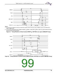
tWC
Address
tCW(2)
tWR(4)
CS1#
tAW
CS2
tCW(2)
tBW
UB#, LB#
tWP(1)
WE#
tAS(3)
tDW
Data Valid
tDH
High-Z
High-Z
Data in
tWHZ
tOW
Data out
Data Undefined
Figure 35. Timing Waveform of Write Cycle(1) (WE# controlled, if BYTE# is Low, Ignore UB#/LB# Timing)
March 31, 2005 S71GL032A_00_A0
S71GL032A Based MCPs
99

 SPANSION [ SPANSION ]