A d v a n c e I n f o r m a t i o n
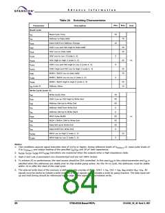
Table 26. Switching Characteristics
Min
Max
Parameter
Read Cycle
Description
Unit
tRC
Read Cycle Time
70
10
tAA
Address to Data Valid
70
tOHA
Data Hold from Address Change
CE#1 Low and CE2 High to Data Valid
OE# Low to Data Valid
tACE
70
35
tDOE
tLZOE
tHZOE
tLZCE
tHZCE
tDBE
OE# Low to Low Z (note 2, 3)
5
5
OE# High to High Z (note 2, 3)
CE#1 Low and CE2 High to Low Z (note 2, 3)
CE#1 High and CE2 Low to High Z (note 2, 3)
BHE# / BLE# Low to Data Valid
BHE# / BLE# Low to Low Z (note 2, 3)
BHE# / BLE# High to High Z (note 2, 3)
Address Skew
25
ns
25
70
tLZBE
tHZBE
tSK (note 4)
5
25
10
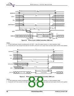
Write Cycle (note 5)
tWC
tSCE
tAW
Write Cycle Time
70
55
55
0
CE#1 Low an CE2 High to Write End
Address Set-Up to Write End
Address Hold from Write End
Address Set-Up to Write Start
WE# Pulse Width
tHA
tSA
0
tPWE
tBW
55
55
25
0
ns
BLE# / BHE# LOW to Write End
Data Set-up to Write End
tSD
tHD
Data Hold from Write End
tHZWE
tLZWE
WE# Low to High Z (note 2, 3)
WE# High to Low Z (note 2, 3)
25
5
Notes:
1. Test conditions assume signal transition time of 1V/ns or higher, timing reference levels of VCC(typ.) /2, input pulse levels of
0 to VCC(typ.), and output loading of the specified IOL/IOH and 30 pF load capacitance.
2. tHZOE, tHZCE, tHZBE and tHZWE transitions are measured when the outputs enter a high-impedance state.
3. High-Z and Low-Z parameters are characterized and are not 100% tested.
4. To achieve 55-ns performance, the read access should be CE# controlled. In this case tACE is the critical parameter and tSK is
satisfied when the addresses are stable prior to chip enable going active. For the 70-ns cycle, the addresses must be stable
within 10 ns after the start of the read cycle.
5. The internal write time of the memory is defined by the overlap of WE#, CE#1 = VIL, CE2 = VIH, BHE and/or BLE =VIL. All
signals must be Active to initiate a write and any of these signals can terminate a write by going Inactive. The data input set-
up and hold timing should be referenced to the edge of the signal that terminates write.
84
S71GL032A Based MCPs
S71GL032A_00_A0 March 31, 2005

 SPANSION [ SPANSION ]