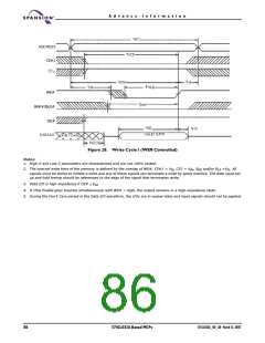
A d v a n c e I n f o r m a t i o n
Maximum Ratings
(Above which the useful life may be impaired. For user guidelines, not tested)
Storage Temperature . . . . . . . . . . . . . . . . . . . . . . . . . . . . -65°C to +150°C
Ambient Temperature with Power Applied . . . . . . . . . . . . . . . -40°C to +85°C
Supply Voltage to Ground Potential . . . . . . . . . . . . . . . . . . . . . -0.4V to 4.6V
DC Voltage Applied to Outputs in High-Z
State (note 1, 2, 3) . . . . . . . . . . . . . . . . . . . . . . . . . . . . . . . . -0.4V to 3.7V
DC Input Voltage (note 1, 2, 3) . . . . . . . . . . . . . . . . . . . . . . . . -0.4V to 3.7V
Output Current into Outputs (Low). . . . . . . . . . . . . . . . . . . . . . . . . . . 20 mA
Static Discharge Voltage. . . . . . . . . >2001V (per MIL-STD-883, Method 3015)
Latch-up Current . . . . . . . . . . . . . . . . . . . . . . . . . . . . . . . . . . . . . >200 mA
Notes:
1. VIH(MAX) = VCC + 0.5V for pulse durations less than 20 ns.
2. VIL(MIN) = –0.5V for pulse durations less than 20 ns.
3. Overshoot and undershoot specifications are characterized and are not 100% tested.
Operating Range
Ambient Temperature (TA)
VCC
-25°C to +85°C
2.7V to 3.3V
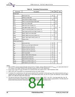
Table 25. DC Electrical Characteristics (Over the Operating Range)
Typ.
(note 1)
Parameter
VCC
Description
Supply Voltage
Test Conditions
Min.
Max
Unit
2.7
3.3
VOH
VOL
VIH
VIL
IIX
Output High Voltage
Output Low Voltage
Input High Voltage
Input Low Voltage
IOH = –1.0 mA
VCC - 0.4
IOL = 0.1 mA
0.4
V
0.8 * VCC
VCC + 0.4
F = 0
-0.4
-1
0.4
+1
+1
15
3
Input Leakage Current
Output Leakage Current
GND ≤ VIN ≤ VCC
µA
IOZ
GND ≤ VOUT ≤ VCC, Output Disabled
-1
f = fMAX = 1/tRC
f = 1 MHz
VCC = 3.3V
IOUT = 0 mA
CMOS Levels
TBD
ICC
VCC Operating Supply Current
mA
CE# ≥ VCC – 0.2V, CE2 ≤ 0.2V
VIN ≥ VCC – 0.2V, VIN ≤ 0.2V,
f = fmax (Address and Data Only),
f=0 (OE#, WE#, BHE# and BLE#)
Automatic CE# Power-Down
Current—CMOS Inputs
ISB1
250
40
µA
CE# ≥ VCC – 0.2V, CE2 ≤ 0.2V
VIN ≥ VCC – 0.2V or VIN ≤ 0.2V,
f = 0, VCC = 3.3V
Automatic CE# Power-Down
Current—CMOS Inputs
ISB2
Notes:
1. Typical values are included for reference only and are not guaranteed or tested. Typical values are measured at VCC
CC(typ.), TA = 25°C.
=
V
82
S71GL032A Based MCPs
S71GL032A_00_A0 March 31, 2005

 SPANSION [ SPANSION ]