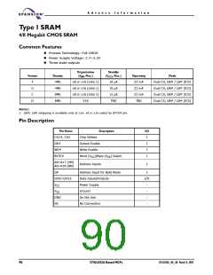
A d v a n c e I n f o r m a t i o n
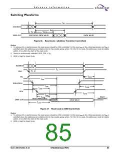
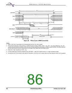
Figure 28. Write Cycle 1 (WE# Controlled)
Notes:
1. High-Z and Low-Z parameters are characterized and are not 100% tested.
2. The internal write time of the memory is defined by the overlap of WE#, CE#1 = VIL, CE2 = VIH, BHE and/or BLE =VIL. All
signals must be Active to initiate a write and any of these signals can terminate a write by going Inactive. The data input set-
up and hold timing should be referenced to the edge of the signal that terminates write.
3. Data I/O is high impedance if OE# ≥ VIH
.
4. If Chip Enable goes Inactive simultaneously with WE# = High, the output remains in a high-impedance state.
5. During the Don’t Care period in the Data I/O waveform, the I/Os are in output state and input signals should not be applied.
86
S71GL032A Based MCPs
S71GL032A_00_A0 March 31, 2005

 SPANSION [ SPANSION ]