A d v a n c e I n f o r m a t i o n
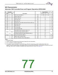
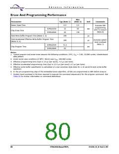
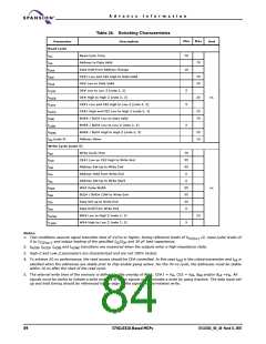
Erase And Programming Performance
Max
Parameter
Typ (Note 1)
(Note 2)
Unit
Comments
Sector Erase Time
0.5
32
3.5
64
Excludes 00h
programming
prior to erasure
(Note 6)
S29GL032A
S29GL064A
sec
Chip Erase Time
64
128
Total Write Buffer Program Time (Notes 3, 5)
240
µs
µs
Total Accelerated Effective Write Buffer Program Time
(Notes 4, 5)
Excludes system
level overhead
(Note 7)
200
S29GL032A
S29GL064A
31.5
63
Chip Program Time
sec
Notes:
1. Typical program and erase times assume the following conditions: 25°C, V = 3.0V, 10,000 cycles; checkerboard
CC
data pattern.
2. Under worst case conditions of 90°C; Worst case V , 100,000 cycles.
CC
3. Effective programming time (typ) is 15 µs (per word), 7.5 µs (per byte).
4. Effective accelerated programming time (typ) is 12.5 µs (per word), 6.3 µs (per byte).
5. Effective write buffer specification is calculated on a per-word/per-byte basis for a 16-word/32-byte write buffer
operation.
6. In the pre-programming step of the Embedded Erase algorithm, all bits are programmed to 00h before erasure.
7. System-level overhead is the time required to execute the command sequence(s) for the program command. See
Table 22 for further information on command definitions.
80
S71GL032A Based MCPs
S71GL032A_00_A0 March 31, 2005

 SPANSION [ SPANSION ]