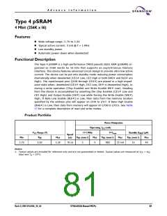
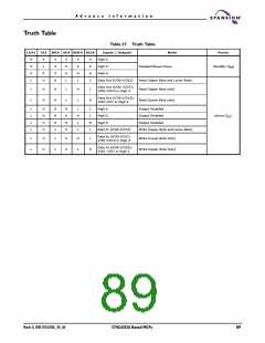
A d v a n c e I n f o r m a t i o n
Switching Waveforms
t
RC
ADDRESS
DATA OUT
t
AA
t
t
SK
OHA
PREVIOUS DATA VALID
DATA VALID
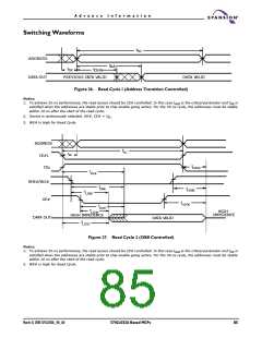
Figure 26. Read Cycle 1 (Address Transition Controlled)
Notes:
1. To achieve 55-ns performance, the read access should be CE# controlled. In this case tACE is the critical parameter and tSK is
satisfied when the addresses are stable prior to chip enable going active. For the 70-ns cycle, the addresses must be stable
within 10 ns after the start of the read cycle.
2. Device is continuously selected. OE#, CE# = VIL.
3. WE# is High for Read Cycle.
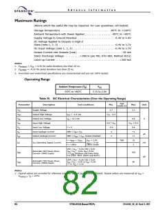
ADDRESS
tRC
tSK
CE#1
tHZCE
CE
2
tACE
BHE#/BLE#
OE#
tDBE
tHZBE
t
LZBE
tHZOE
tDOE
t
HIGH
LZOE
IMPEDENCE
HIGH IMPEDENCE
DATA OUT
DATA VALID
t
LZCE
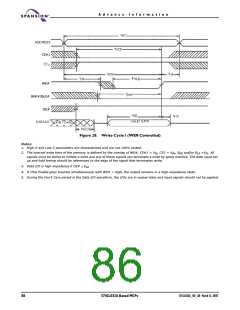
Figure 27. Read Cycle 2 (OE# Controlled)
Notes:
1. To achieve 55-ns performance, the read access should be CE# controlled. In this case tACE is the critical parameter and tSK is
satisfied when the addresses are stable prior to chip enable going active. For the 70-ns cycle, the addresses must be stable
within 10 ns after the start of the read cycle.
2. WE# is High for Read Cycle.
March 31, 2005 S71GL032A_00_A0
S71GL032A Based MCPs
85

 SPANSION [ SPANSION ]