A d v a n c e I n f o r m a t i o n
Type 4 pSRAM
4 Mbit (256K x 16)
Features
Wide voltage range: 2.7V to 3.3V
Typical active current: 3 mA @ f = 1 MHz
Low standby power
Automatic power-down when deselected
Functional Description
The Type 4 pSRAM is a high-performance CMOS pseudo static RAM (pSRAM) or-
ganized as 256K words by 16 bits that supports an asynchronous memory
interface. This device features advanced circuit design to provide ultra-low active
current. The device can be put into standby mode reducing power consumption
dramatically when deselected (CE1# Low, CE2 High or both BHE# and BLE# are
High). The input/output pins (I/O0 through I/O15) are placed in a high-imped-
ance state when: deselected (CE1# High, CE2 Low, OE# is deasserted High), or
during a write operation (Chip Enabled and Write Enable WE# Low). Reading
from the device is accomplished by asserting the Chip Enables (CE1# Low and
CE2 High) and Output Enable (OE#) Low while forcing the Write Enable (WE#)
High. If Byte Low Enable (BLE#) is Low, then data from the memory location
specified by the address pins will appear on I/O0 to I/O7. If Byte High Enable
(BHE#) is Low, then data from memory will appear on I/O8 to I/O15. See Table
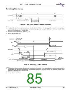
27 for a complete description of read and write modes.
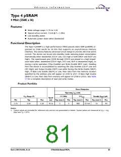
Product Portfolio
Power Dissipation
Operating, ICC (mA)
f = 1 MHz f = fmax
Typ. (note 1) Typ. (note 1)
TBD
VCC Range (V)
Typ
Standby (ISB2) (µA)
Speed
(ns)
Min
Max
Max
Max
Typ. (note 1)
Max
2.7V
3.0V
3.3V
70 ns
3
5
25 mA
15
40
Notes:
1. Typical values are included for reference only and are not guaranteed or tested. Typical values are measured at VCC = VCC
(typ) and TA = 25°C.
March 31, 2005 S71GL032A_00_A0
S71GL032A Based MCPs
81

 SPANSION [ SPANSION ]