A d v a n c e I n f o r m a t i o n
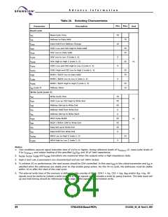
tWC
ADDRESS
CE#1
tSCE
CE2
tBW
tAW
BHE#/BLE#
tHA
tSA
t
PWE
WE#
t
HD
tSD
DON’T CARE
DATA I/O
VALID DATA
t
tHZWE
LZWE
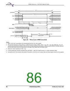
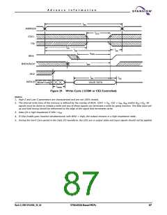
Figure 30. Write Cycle 3 (WE# Controlled, OE# Low)
Notes:
1. If Chip Enable goes Inactive simultaneously with WE# = High, the output remains in a high-impedance state.
2. During the Don’t Care period in the Data I/O waveform, the I/Os are in output state and input signals should not be applied.
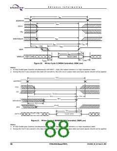
CE#1
CE2
BHE#/BLE#
WE#
Figure 31. Write Cycle 4 (BHE#/BLE# Controlled, OE# Low)
Notes:
1. If Chip Enable goes Inactive simultaneously with WE# = High, the output remains in a high-impedance state.
2. During the Don’t Care period in the Data I/O waveform, the I/Os are in output state and input signals should not be applied.
88
S71GL032A Based MCPs
S71GL032A_00_A0 March 31, 2005

 SPANSION [ SPANSION ]